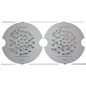
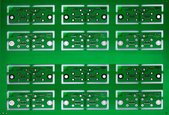
Large & Small PCB


Nowadays, the reduction of the size of the basic printed circuit board supplierwill reach half or the quarter of the original size. The extremely thin wires that designers couldn't use before are now the mainstream, and the thinnest wire with 75 micrometers (3 mils) has gradually been reduced to 30 micrometers (1.2 mils) or even thinner.
Manufacturers of a sophisticated small printed circuit boardcan be divided into four groups. The first group is in the Asian area, which has developed the unique thin wire process for s or iPods and can arrange wires of 40-50 micrometers. The second group consists of the research and development companies of limited numbers which produce small numbers of very professional circuits with thin wires of less than 40 micrometers.
The third group is expanding its business of large PCB boardand medium-sized PCB board with the highest speed. They provide a little output with wires of 75-40 micrometers in width, and they can produce several thousand within weeks. At last, the fourth group produce mini PCB board, micro PCB board, mic PCB boardnormally with the wires of 125-75 micrometers and includes a large number of manufacturers and participants.
As the microelectronics business expands, more and more PCB companies find out the necessary technology in producing the very thin wires with a width of 40 micrometers, and even less than it, circuit designers need to be familiar with the new design rules and the merits and demerits of microelectronics manufacturing.
PCB Design Service:
All kinds of PCB design service including multilayer, rigid, flexible, and rigid-flexible PCB
Easily accomplish the sophisticated and concentrated PCB layout design
Advanced component packaging and library creation, including BGA, QFN packaging
High-speed PCB design, including differential pairs, length matching, etc.
High expertise in critical and sensitive signal routing in analog and digital circuits
PCB Reverse Engineering Service
Redesign services to correct defects or optimize existing PCB designs to reduce costs
PCB model making
PCB manufacturing
PCB design testing service
As a pcb board supplier,we are looking forward your callings.
Send product request
Other supplier products
 |
IMMERSION SILVER PCB - PRINTED CIRCUIT BOARD | The immersion silver process of immersion silver pcbmanufacturing is between OSP and immersion nickel / gold, and the process is relatively simple ... |
 |
OSP PCB - PRINTED CIRCUIT BOARD | OSP differs from other surface treatment processes in that it functions as a barrier layer between copper and air; in short, OSP is a chemically gr... |
 |
LEAD FREE HASL PCB / IMMERSION TIN PCB | LEAD FREE HASL PCB / immersion tin pcb Lead-free HASL is to coat a layer of tin-lead alloy on the copper surface to prevent the oxidation of the co... |
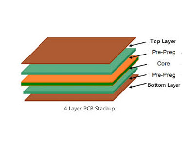 |
4 Layer PCB | In general, in a 4 layer pcb layout, both the top and bottom layers belong to the signal layer, while another two inner layers are GND and VCC. If ... |
 |
WIRING ON THE DOUBLE-SIDED BOARD——DOUBLE SIDED PCB | Speedapcb - The printed circuit board manufacturersin China, established in 2014, is located in Changsha, Hunan Province. The company focuses on hi... |