

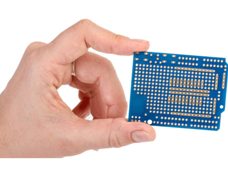
Blind Via PCB


ZF Electronics was founded in 2003, headquartered in Shenzhen China, the world's most complete electronic supply chain. ZF electronics has been one of theprofessional pcb manufacturing companies, from prototype to mass production. Our process includes recommending customers to select easy-to-purchase p/n components in the design stage of a new project and purchasing all electronic components, PCB manufacture, PCBmanufacturing assembly, testing, and fast delivery to our customers.
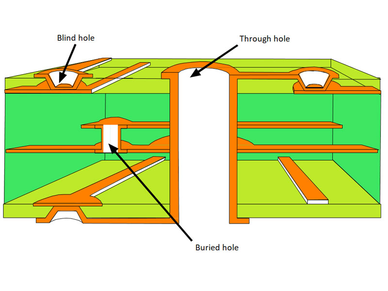
As the name suggests, blind via buried viacannot be seen. Blindvia in pcbis the via that connects the surface layer and the inner layer without penetrating the entire board. In order to increase the space utilization of the PCB circuit layer, the blind via is produced. Blind via is located on the top and bottom surfaces of the printed circuit board and has a certain depth. It is used to connect the surface circuit and the underlying inner circuit and the depth of the hole usually does not exceed a certain blind via aspect ratio(aperture).
How to manufacture blind via PCB?
The blind via PCB production method requires special attention to the depth of the drilling (Z-axis) to be just right. If you do not pay attention to it, it will cause difficulties in electroplating in the via, so almost no factory adopts it. You can also put the circuit layer that needs to be connected in advance in the individual circuit layer. The hdi viasare drilled first, and then glued together, but more precise positioning and alignment devices are required.
The line width and line spacing of most process equipment: blind via 0.1mm, 0.125mm, 0.15mm.
Difference between blind via and plating through hole PCB
From the processing point of view,through hole circuit boardPCB and blind via holePCB have different requirements for cutting tools in terms of chip removal ability. The processing of blind buried viasmakes it easy for the cutting tool to be buried in iron chips, so better chip removal performance is required.
It is better to use spiral flute taps to machine blind holes, instead of straight flutes, it is easy to block chips and cause tool breakage.
For drilling and blind hole processing, it is best to use an internally cooled central water outlet drill bit. With the central water outlet effect of the machine tool, the iron filings can be forced off by the coolant pressure, so that the iron filings will not be entangled and blocked, which leads to over-tolerance in machining and breakage of tools.
The boring is the same as the drilling, and it is best to use the center outlet.
But the above statement is not absolute espeically when you wantcustom made pcb boards. It mainly depends on the depth-to-diameter ratio of the blind via. If the shallow hole is processed, it can also be used as a general plating through hole PCB processing tool.
If you have questions about our blind via PCB production capacity, or the specifications required for your custom project are not listed on this page, please feel free to contact us. We will reply within one workday. We will continue to provide quotation support and design support. Welcome to learn about our production process.
Other PCB Fab
Related Videos
Leave a Message
PCB Market
Related News
FAQs
How to Get a Quotation for PCBA (Assembly PCB)?
Please send BOM(Bill of Material/Components) and above mentioned PCB files. It’s better if you could supply finished production photos and full requirement detail images.
What will need for PCB clone service?
Please send us the printed circuit board concerned,and also the sharp photos of its front side and the back side.
在线联系供应商
Other supplier products
 |
Multilayer PCB | ZF Electronics, as one of the top pcb fabrication companiesin China, can provide customers with single-sided PCB, double-sided FR4 PCB, metal core ... |
 |
Multilayer PCB | Printed circuit board (PCB) now plays the most important role in electronic products. The PCB used in the past was very simple and limited to a sin... |
 |
Thick Copper PCB | PCBs are usually bonded to a layer of copper foil on a glass epoxy substrate, the thickness of which is usually 18μm, 35μm, 55μm and 70&mu... |
 |
Thick Copper PCB | ZF Electronics, as one of the top pcb assembly supplierin China, can provide customers with single-sided PCB, double-sided FR4 PCB, metal core PCB,... |
 |
Rigid PCB | PCB can be divided into rigid PCB and flexible PCB according to the production materials. The rigid PC boardcontains phenolic paper laminate, epoxy... |
Same products
 |
C500-1.7 Series High Flow Multi-Stage Centrifugal Blower /Centrifugal Blower | 卖方: Greentech International (Zhangqiu) Co., Ltd | Greentech International (Zhangqiu) Co., Ltdis the professional blower supplier.Multistage Centrif... |
 |
Common Rail injector control valve F00VC01303 | 卖方: China Lutong Part Plant | Common Rail injector control valve F00VC01303 Tina#Stainless Steel Cylindrical Pin##Denso Common... |
 |
Common Rail injector control valve F00VC01200 | 卖方: China Lutong Part Plant | Common Rail injector control valve F00VC01200 Tina#Stainless Steel Cylindrical Pin##Denso Common... |
 |
Injector Control Valve Plate 24# | 卖方: China Lutong Part Plant | Injector Control Valve Plate 24# Tina#Stainless Steel Cylindrical Pin##Denso Common Rail Injecto... |
 |
Injector Control Valve Plate 12# | 卖方: China Lutong Part Plant | Injector Control Valve Plate 12# Tina#Stainless Steel Cylindrical Pin##Denso Common Rail Injecto... |
