
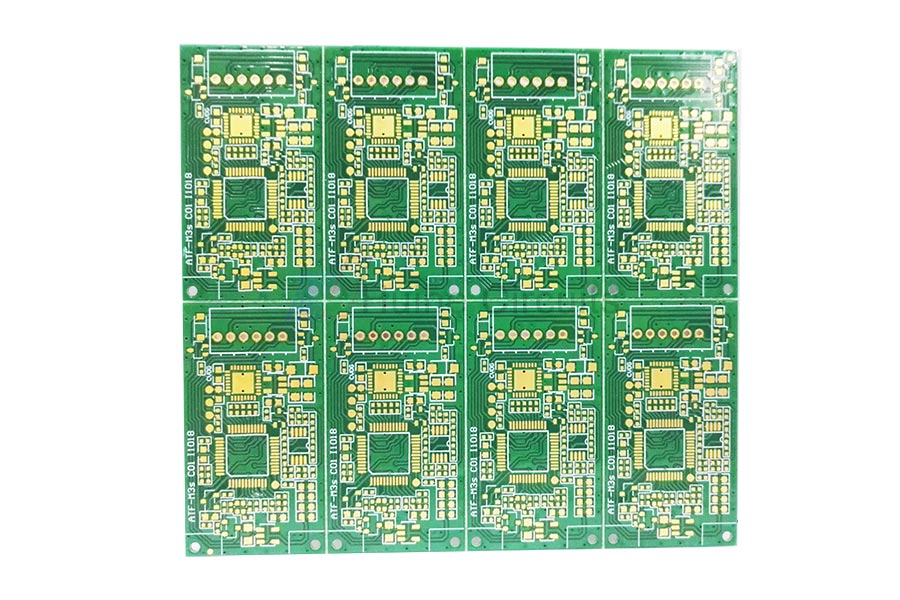
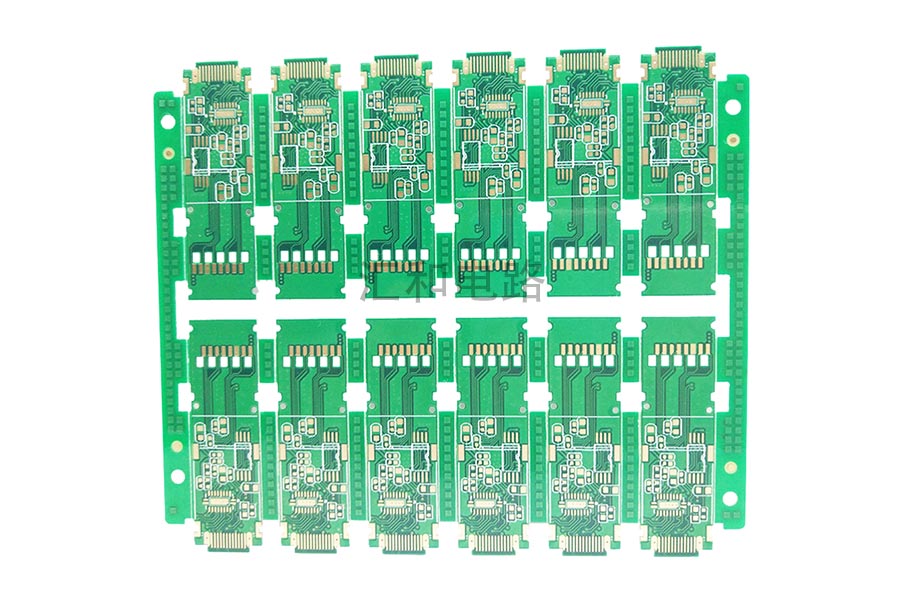
Half Hole & Through Hole Pcb


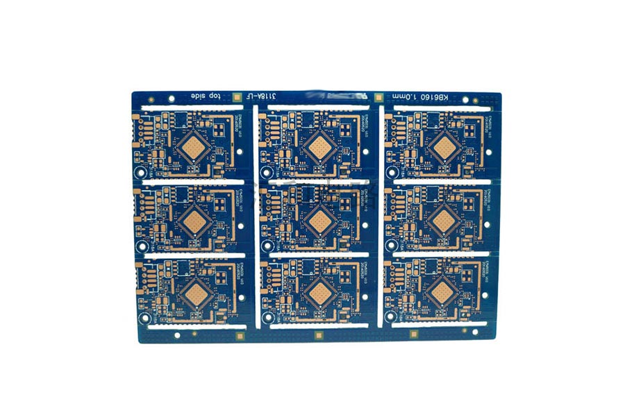
Half Hole & through hole circuit board, no copper burr residue or warpage in half hole, reduce connectors and save space, apply to Bluetooth module and Signal receiver products. HUIHE CIRCUITS Half Hole & Through Hole PCB, apply to Bluetooth module and Signal receiver products. Has passed ISO9001 / ISO13485 /IATF16949 / UL /RoHS / REACH certification.
Half Hole & Through Hole PCB List
2 Layer OSP Impedance Control Half Hole PCB
2 Layer ENIG Half Hole PCB
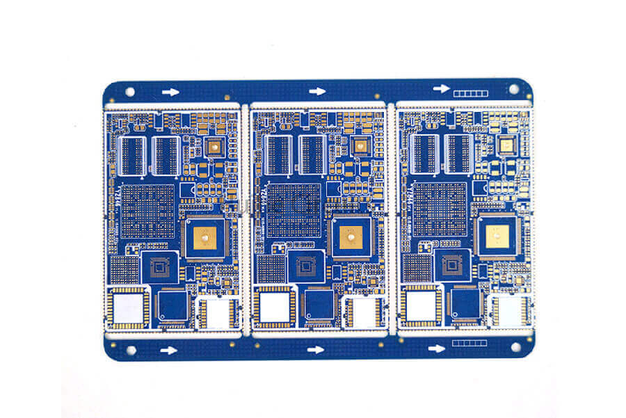
4 Layer ENIG Impedance Control Half Hole PCB Electric Circuit Board
2 layer ENIG impedance control half hole pcb
8 layer ENIG half hole custom PCB
4 layer ENIG impedance control half hole fr4 PCB
4 layer ENIG impedance control half hole PCB
4 layer LF-HASL half hole PCB
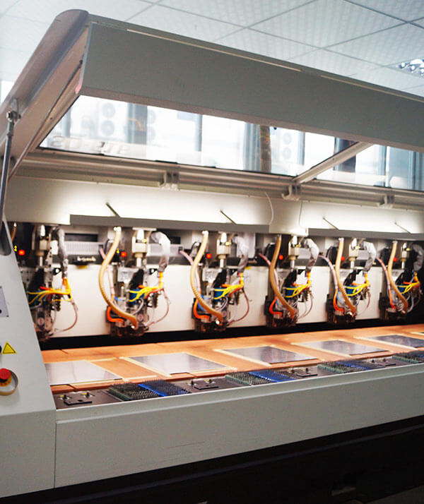
Production Process Of Metallized Half-Hole PCB
For the front inversion, to prevent the quality of the product and the need to make corrections in the later process, the production process of this type of board is processed according to the following process: a drilling (drilling, gong groove-plate surface plating-external Optical imaging-pattern plating-co-drying-half-hole processing-film stripping, etching, tin stripping-other processes-shape
Main Points Of Metallized Half-Hole PCB Production
The specific metallized half-holes are processed in the following way: all metallized half-hole PCB holes must be drilled in the pattern after plating, and one hole at the intersection of the two ends of the half-hole should be drilled before etching.
The engineering department formulates the MI process according to the process
The metal half-hole is the second-drilled half-hole drilled during the first drilling (or gong), after the image is plated, and before the etching. It is necessary to consider whether the copper will be exposed when the gong groove is shaped, and move the drilled half-hole into the unit.
he right hole is drilled first, and then the board is turned over (or mirrored) and the left hole is drilled to reduce the pulling of the copper of the inner hole of the half hole by the drill, resulting in the lack of copper of the hole.
The size of the drill nozzle for drilling the half hole depends on the spacing of the contour lines.
Draw the solder mask film, use the gong space as a stop point and open the window to increase 4mil treatment.
The Designer's Suggestion When Designing The Circuit
Change the distance from the edge line to the hole center. The general design is to place the hole center on the edge line and move the control center down. For example, the diameter of the hole is 1.4mm, the distance between the two holes is 2.54mm, and the board edge The distance between the line is 0.33mm from the center of the through hole, and the thickness of the plate is 0.6mm. The angle between the tangent to the cut point of the wall and the track of the milling cutter was 90 degrees before, but this time it is about 60 degrees. Because the board edge line is at a certain distance from the center of the through hole, the cutting angle of the milling cutter is changed, and the board thickness is extremely small, so the copper in the hole is not easily pulled out. The simultaneous improvement of small batch pcb design and production can greatly improve the production yield of pcb board with holes.
In our circuit board factory, we have types of pcb boardfor sale, if you have needs, please contact us.
在线联系供应商
Other supplier products
 |
New Energy PCB | As aprofessionalpcb manufacturing company, HUIHE Circuits has mastered advanced technology in the PCBindustry, we own reliable production equipment... |
 |
Internet Of Things PCB | Blind and buried via PCBs used in IoT devices can place dense electronic components and flexible wiring.Blind and buried vias circuit boards use bl... |
 |
Rail Transit PCB | Huihe Circuits has extensive experience in manufacturing customized subway pcbfor customers in the railway, rail transit and automotive industries.... |
 |
4 Layer FR4+Rogers ENIG PCB | Number of layers: 4 size:80*88mm Surface finish: ENIG Base material: Rogers FR4 4350B Min. hole diameter: 0.3mm Minimum Line Width:0.230mm Minimum ... |
 |
4 Layer ENIG Impedance Control Half Hole PCB Electric Circuit Board | Number of layers: 4 Surface finish: ENIG Base material: FR4 Outer Layer W/S: 6/4mil Inner layer W: 21mil Thickness: 0.4mm Special process: im... |
Same products
 |
LW34-12 10KV outdoor SF6 circuit breaker | 卖方: Bokong Electric Co., Ltd | Product Description LW34-12 10KV is a new outdoor high-voltage electrical arcing and SF6 gas a... |
 |
Consumer PCB | 卖方: Xinfeng Huihe Circuits Co., Ltd. | The size, thickness and weight of products in the consumer electronics field have been greatly re... |
 |
PCB Prototyping | 卖方: Xinfeng Huihe Circuits Co., Ltd. | China high quality pcb prototypeFactory Has 97% On-Time Delivery Ratio In accordance with IPC st... |
 |
PCB Application | 卖方: Xinfeng Huihe Circuits Co., Ltd. | PCB Application As a leading PCB supplier in China printed circuit board industryincluding com... |
 |
PCB Board For Sale | 卖方: Xinfeng Huihe Circuits Co., Ltd. | With the help of a technology development team for professional printed circuit board manufacture... |