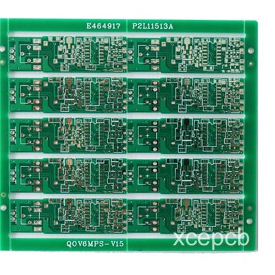
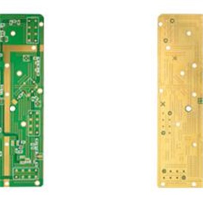
Hole Copper 25um 8 Layer Pcb Board With Hole In Pad Electronic Panels


Hole copper 25um 8 layer pcb board with hole in pad electronic panels • Do you have an order minimum?1pc or 1 panel acceptable,also for PCBA.• How to place the order?After we quote for you,and you will accept the price,then we will send proforma invoice to you for payment,also you can contact us by .• What kind of transportation we adopt? It'll depand on your choice.Most time we will delivery on DHL or Fedex IP,if you have requirements for the delivery way,we will according to your choice. Xinchenger Electronics co.,Ltd established in 2002,we have commited ourselves to manufacturing various of hi-frequency microwave pcb and multi-layer board including fastest sample production. we have accumulated abandunt experiences in the line of high frequency microwave business for which widely apply to power divider,combiner,power amplifier,line amplifier,base station,RF antena,4G antena so on and so forth.our company's sufficient stocks of hi-frequency pcb materials such as Rogers,TACONIC,Arlon,Isola,F4B,TP-2,FR-4 (dielectric rage:2.2-16) mainly used in the area of high technologies like communication device,Electronics,Aerospace,Military industry to meet our worldwide customers with high quality.furthermore,we also keen on helping customers shorten the period of production development and 24 hours of sample service is available. Since the day of company foundation we continuously enaged in researching special and high precision printed circuit boards with the strong production capability of 2 to 28 layers of highly precise impedence,multi-layer blind buried,multi-layer mix-compression,highTG, copper substrate,Ceramic substrate PCB.we emphasize the significance of traning program for every single staff in the company even grass-roots employees which becomes the most competitive factors to excel from others,our company have many experienced and professional teams from management to production line,30% are highly educated among the total amount of employees,advanced engineers and senior technicians are up to 80 people. With advanced foreign technology supports and domestic 3G/4G device manufacturer in microwave pcb field which lead our experienced hi-frequencey researching team to one step ahead of the line of printed circuit board business,we are hornored to obtain sound reputations over our wolrdwide customers on the basis of fine qulity,prompt delivery,satisfied after sales service for may years and we assure our customers that we will return the favors with more and more superior products in the near future. Intraday hole is an important part of a multi-layer PCB, which not only bears PCB main function performance, and drilling costs are generally 30% to 40% PCB system board costs. In short, each hole on the PCB can be called pan holes. From the role of point of view, intraday holes can be divided into two categories:One is used for electrical connection between the layers; the second is used as a device for fixing or positioning. If from the process technology, these disk holes are generally divided into three categories, namely blind holes (blind via), buried vias (buried via) and through-hole (through via). Blind holes located on the top and bottom surfaces of the printed circuit board, having a certain depth, the line for connecting the surface layer and the inner layer below the line, the depth of the hole is usually no more than a certain ratio (aperture). Buried hole printed circuit board means located in the inner connection hole, it does not extend to the surface of the board. These two types of holes are located in the inner layer circuit board, laminated before use through-hole forming process is completed, the through-hole forming process may also overlap several good lining. The third is called through-hole, this hole through the entire circuit board can be used to implement the interconnect or installed as locating hole components. Since the through-holes in the process easier to implement, low cost, so most of the printed circuit boards are to use it, rather than the other two plate holes. Company Service:24 hours quick sample is avaliable here.reply Customer's any enquiry within 3 hours;Blind buried hole ,crossed blind hole can be done24 hours Engineering Gerber files treatment.24 hours English Engineering Questions Confirmation by E-mail.Supply the best project fit for production customized Model Number:XCEPCB0019 Shipping port:ShenZhen/HongKong Place of origin:GuangDong,China Delivery Time:3-10 Working Days Production capacity:FR4:2000000Sqms High Frequency board:10000SqmsPrice Terms:FOBMinimum Order Quantity:1pcPayment terms:TT,Paypal,Western UnionCertification:CE,ROHS,FCC,ISO9008,SGS,ULMaterial:FR4Soldermask:GreenMolde Number:xcepcb0019Silkscreen:WhiteLayer:8Panel Size:105*125mm/5pcsBoard Thickness:1.0mmPackage Details:Inner:Vacuum-packed Bubble bag With Foam Outer:Carton BoxMin Line Space:4MilMin Line Width:4MilMin Hole Size:10MilFinished Surface:ENIGSpecial requirement:BGAcopper 25umProvide Slice reportFinished Copper:1ozDelivery Time:8 DaysBGA stands for Ball Grid Array (PCB ball grid array structure), which is an integrated circuit using an organic carrier board an encapsulation method. It has: ① ② reduce package size function to increase the number of pins increases ③PCB board is dissolved welding self-centered, easy on the tin ④ ⑤ good electrical performance, high reliability, and low overall cost. BGA PCB board has more holes in general, most customers BGA lower through-bore design for the finished hole diameter 8 ~ 12mil, BGA surface at a distance from the hole to fit specifications for 31.5mil for example, is generally not less than 10.5mil. BGA vias required under the plug hole, BGA pads are not allowed on the ink, not drilling on the BGA pads. Parameter:oItemData1Layer:1 to 24 layers2Material type:FR-4, CEM-1, CEM-3, High TG, FR4 Halogen Free, Rogers3Board thickness:0.20mm to 3.4mm4Copper thickness:0.5 OZ to 4 OZ5Copper thickness in hole:>25.0 um (>1mil)6Max. Board Size: (580mm×1200mm)7Min. Drilled Hole Size:4mil(0.1mm)8Min. Line Width:3mil (0.075mm)9Min. Line Spacing:3mil (0.075mm)10Surface finishing:HASL / HASL lead free, HAL, Chemical tin, Chemical Gold, Immersion Silver/Gold, OSP, Gold platingMaximum PCB Size2 Layer 20" x 28"Mulitlayer 16" x 26"Minimum Conductor Space0.003"Minimum Conductor Width0.003"Minimum Drill Hole Size0.006"Finish Plating / Surface FinishesHASL – Leaded Solder Tin/NickelHASL – Lead Free SolderElectroless Soft GoldWire Bondable Soft GoldNickel Flash GoldElectroless NickelImmersion Gold OSPElectrolytic Nickel /Hard Gold and Selective GoldImmersion SilverImmersion TinCarbon InkENIGFinished Copper – Outer Layers1oz Cu – Min .004" Trace/Space2oz Cu – Min .005" Trace Space3oz Cu – Min .008" Trace/Space4oz Cu – Min .010" Trace/Space5oz Cu – Min .012" Trace/SpaceWe can manufacture higher ounces of copper depending on the specs. Please let us know how much you would like when sending us your PCB specs.Competitive Advantage:1) With UL,ROHS,ISO,IPC2).Lead time:3-10 working days3)Competitive price best quality4).Rich 20 years experience in High Tg Multilayer PCB . What Information customer need to provide for quotation ?1. PCB Gerber files ,protel,powerpcb,Autocad,etc.2. BOM list for PCB assembly.3. Send us your sample PCB or PCBA.4. OEM is acceptable. Contact Information:Karen-Sales DepartmentShenZhen Xinchenger Electronic
Other supplier products
|
|
F4B Pcb |
Chinese High Frequency PCB Material F4B Laminate Circuit BoardsSpecification:Materia raw F4B high frequencyBoard THK0.6mmLayer6Solder mask... |
|
|
Rogers Rf |
Single Sided Rogers 4003C PCB boards With White Solder Mask Specification:
Number of Layer: 1
Board material: rogers 4003C
Board thickness: 0... |
|
|
Halogen Free Pcb |
Halogen FreeConcerns regarding the health and safety of halogenated flame retardants in PWB applications dates to the early 1990s when it was disco... |
|
|
Rogers 4003 Material |
High Frequency Rogers RO4003CLaminates Typical Applications
High reliability aerospace and defense
A wide range of typical and non-traditional ... |
|
|
Arlon Pcb |
Name: 4 layer high frequency Arlon immersion gold pcb producerMost popular Arlon model:AD255,TC350,Diclad522Quick detail: Layer of number4Surface ... |
All supplier products
Same products