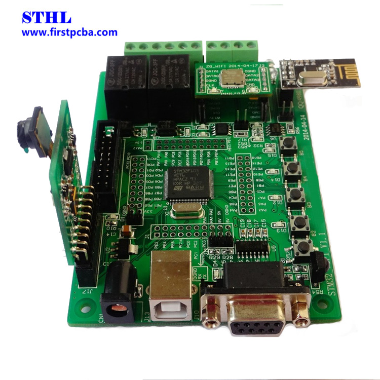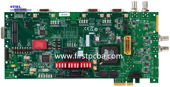
Controlled Impedance 6L/1.6mm HDI PCB in Mobile with blind and buried holes


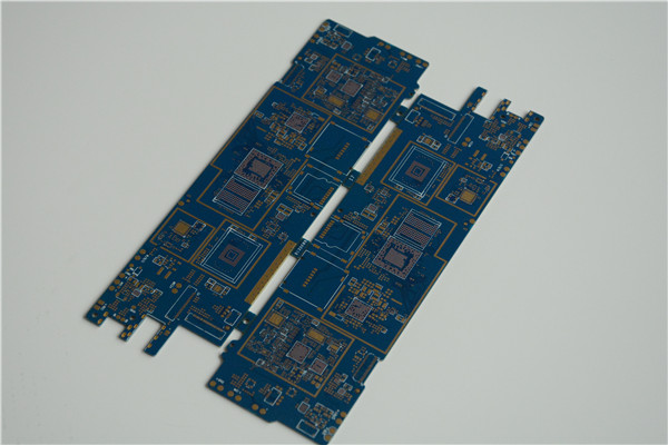
Application Field: Mobile
Layer/Board Thickness:6L/1.6mm
Surface Treatment: ENIG+OSP
Line/Space: 3.5/3.5mil
Smallest Hole Diameter:0.15mm
Technical Feature: 1+4+1, impedance control blind and buried holes
Send product request
Other supplier products
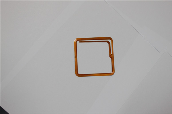 |
High quality Rigid Flex 1L/1.5mm PCB CHINESE factory Manufacturing | Layer/Board Thickness: 1L/1.5mm Surface Treatment: ENIG Line/Space: 10.0/10.0mil Smallest Hole Diameter: 0.3mm Technical Feature: flex PCB |
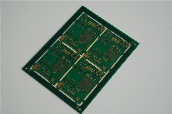 |
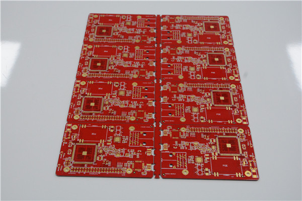
Multilayer PCB Chinese factory Printed Circuit Boards Signal Integrity Simulations | Application Field: Communication Layer/Board Thickness:10L/1.6mm Surface Treatment: ENIG Line/Space: 4/4mil Smallest Hole Diameter:0.2mm Technical ... |
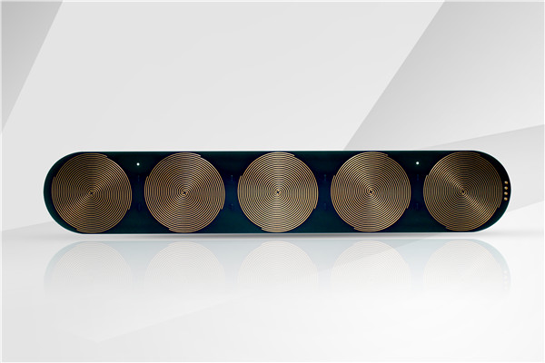 |
Rigid Prototype 2L/1.6mm instruments PCB with Coil pattern circuit | Application Field: Consumer electronics Layer/Board Thickness: 2L/1.6mm Surface Treatment: ENIG2u” Line/Space: 8.0/8.0mil Smallest Hole Diame... |
 |
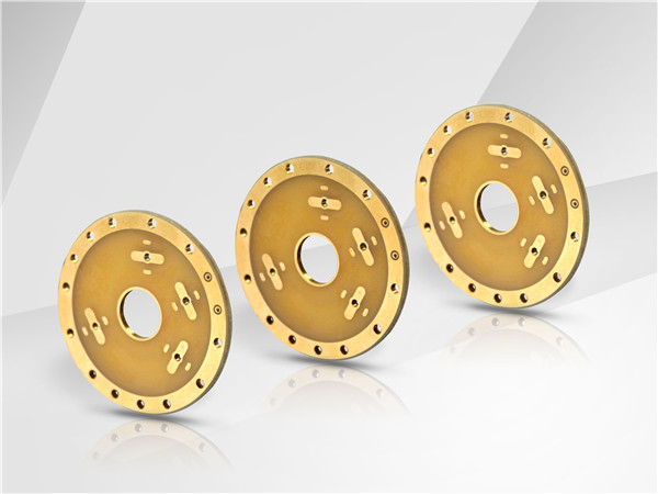
high Low voltage Rigid Heavy Copper PCB for 15 oz heavy copper Power meter | Application Field: Consumer electronics Layer/Board Thickness: 6L/1.6mm Surface Treatment: ENIG3u” Line/Space: 5.0/5.0mil Smallest Hole Diame... |
 |
Rigid 2L/1.6mm Hardware Systems Design PCB in Consumer electronics | Application Field: Consumer electronics Layer/Board Thickness: 2L/1.6mm Surface Treatment: Hard gold 30u” Technical Feature: Hard gold surfac... |