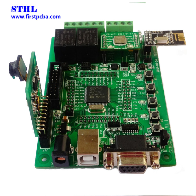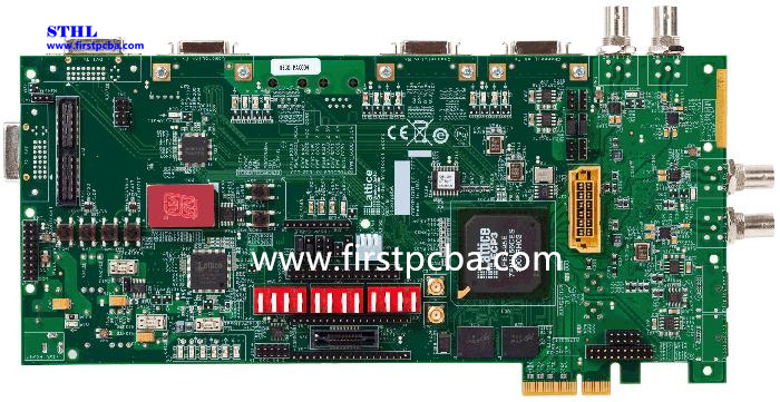
6 Layer ENIG PCB


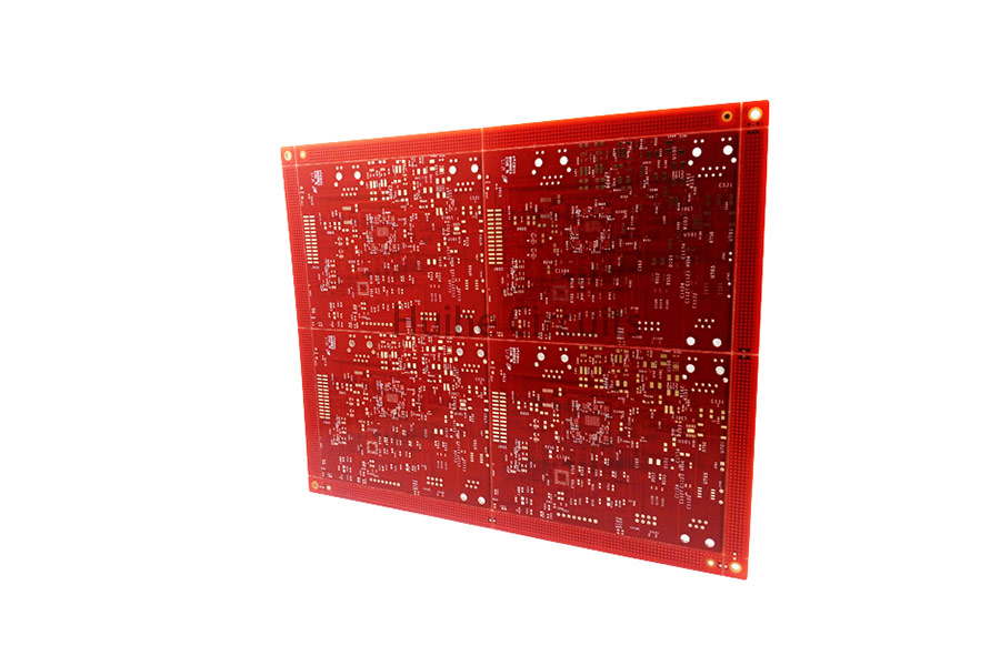
Number of layers: 6
Surface finish: ENIG
Base material: FR4
Outer Layer W/S: 4/2mil
Inner layer W/S: 4/3mil
Thickness: 1.6mm
Advantages Of pcb 6 layer
Own lamination process to convenient production for Multilayer PCB and shorten the lead time.
Jiangxi facility is environmental-friendly approved by the government .
Famous raw materials brand, Kingboard, Shengyi, ITEQ, Taiyo, Guangxin.
Highly automated production line with AIO Optical Scanning, Electroplating Automatic Line, High-speed flying probe test machines and inkjet printer.
Engineers with more than 15 years of experience
Customers located in more than 20 countries, the common choice of 500 high-end companies.
Perfect quality inspection system
Professional R&D team can make all kinds of special boards.
Quick turn, prototype, medium or large batches can be produced to meet the needs of different customers.
Quick response to quotes.
The management level is highly educated, 30% have professional titles and more than ten years of work experience.
High staff stability, low mobility.
UL/ISO9001/SGS/IATF16949/ROHS/ISO1400 certificated.
Sales office in Shenzhen and own 12,000sqm factory in Jiangxi.
Establish an e-commerce system to reduce transaction costs and increase market response speed.
Huihe Circuits is a professional pcb manufacturer, we provide bare printed circuit board, bare pcb board, bare pcb, printed circuit boardand etc. For more information, please feel free to contact us!
Send product request
Other supplier products
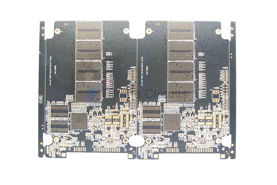 |
Via In Pad Fr4 PCB | Via In pcb board material fr4, using copper plating or epoxy to fill holesfor circuit board factor, prevent solder paste or flux from flowing into ... |
 |
PCB Application | As aprofessionalpcb manufacturing company, HUIHE Circuits has mastered advanced technology in the PCBindustry, we own reliable production equipment... |
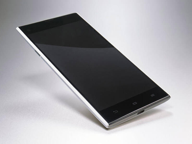 |
Consumer PCB | The size, thickness and weight of products in the consumer electronics field have been greatly reduced. Via in pad PCB, blind buried vias PCB, half... |
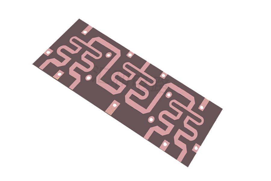 |
2 Layer F4B ENIG PCB | Number of layers: 2 Surface finish: ENIG Base material: F4B Outer Layer W: 6mil Outer layer S: 6mil Thickness: 1.0mm Advantages Of 2 Layer F4... |
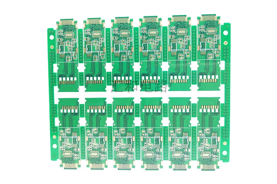 |
4 Layer ENIG Impedance Control Half Hole PCB Electric Circuit Board | Number of layers: 4 Surface finish: ENIG Base material: FR4 Outer Layer W/S: 6/4mil Inner layer W: 21mil Thickness: 0.4mm Special process: im... |