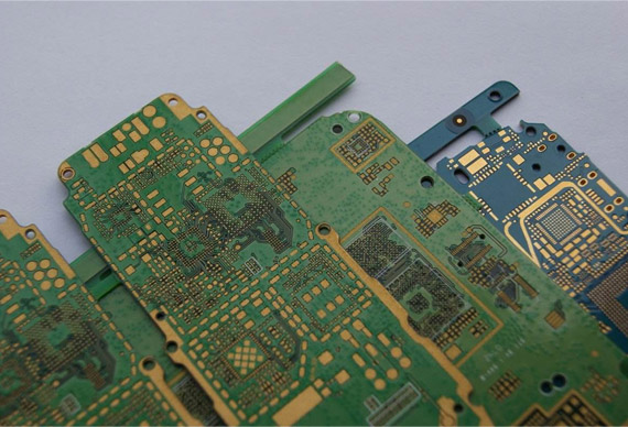
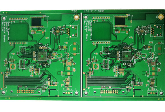
HDI PCB / BLIND&BURIED VIA HOLE PCB / BVH PCB


SPEEDAPCB has been focusing on the production of various PTH (plated through hole PCB), buried via hole PCB and blind via hole PCB, and HDI PCB prototype.
When it comes to blind and buried hole circuit boards, everyone thinks of HDI boards. Generally, there are more blind and buried hole circuit boards used in mobile s or navigation instruments. Such PCB boards require high technical content and accurate accuracy. Of course, the price is compared with other It is also high for multilayer circuit boards.
HDI high density interconnect pcb : 1 + n + 1, 1 + 1 + n + 1 + 1, 2 + n + 2, 3 + n + 3,
Features of Blind&Buried Via Hole PCB
HDI PCB
Blind Via Hole is the connection between the outermost circuit in the PCB and the adjacent inner layer with a plated hole. Because the opposite side cannot be seen, it is called blind pass. In order to increase the space utilization between the circuit layers of the board, blind holes come in handy. The blind hole is a via hole to the surface of the printed board.
Buried Via Hole, the connection between any circuit layers in the PCB, but there is no conduction with the outer layer, that is, there is no meaning of a via hole extending to the surface of the circuit board.
HDI PCB
The blind holes are located on the top and bottom surfaces of the circuit board and have a certain depth. They are used to connect the surface layer circuits to the inner layer circuits below. The depth of the holes generally has a prescribed ratio (aperture). This manufacturing method requires special attention, and the drilling depth must be just right. Failure to pay attention will cause difficulties in plating inside the hole. Therefore, few factories will adopt this production method. In fact, it is possible to drill the holes of the circuit layers that need to be connected beforehand, and then glue them together, but they need more precise positioning and alignment devices.
HDI PCB
This manufacturing process cannot be achieved by bonding the circuit boards and then drilling. It is necessary to perform the drilling operation at the individual circuit layer, firstly locally bond the inner layer, then perform plating treatment, and finally all the bonding. Because the operation process is more laborious than the original vias and blind holes, the price is also the most expensive. This manufacturing process is usually only used for high-density circuit boards, increasing the space utilization of other circuit layers.
HDI PCB
In the PCB manufacturing process, drilling is very important. The simple understanding of drilling is to drill the required via holes on the copper clad board, which has the function of providing electrical connections and fixing devices. If the operation of the via is caused by incorrect operation, the device cannot be fixed on the circuit board, which will affect the use of the circuit board, and the entire board will be scrapped. Therefore, the process of drilling is very important.
Parameters of Blind&Buried Via Hole PCB
|
Items |
||
|
Max board size |
580X700mm |
|
|
Boar Material |
FR-4,Aluminum, High Tg FR4,CEM3,etc. |
|
|
Min trace width/ space (inner layer) |
4mil/4mil(0.1mm/0.1mm) |
|
|
Min PAD (inner layer) |
5 mil(0.13mm) |
|
|
Min thickness(inner layer) |
4 mil(0.1mm) |
|
|
Inner copper thickness |
||
|
Outer copper thickness |
||
|
Finished board thickness |
||
|
Board thickness tolerance control |
±0.10 mm |
±0.10 mm |
|
±10% |
±10% |
|
|
±10% |
±10% |
|
|
Inner layer treatment |
brown oxidation |
|
|
Layer count Capability |
1-30 LAYER |
|
|
alignment between ML |
±2mil |
|
|
Drill hole diameter |
||
|
Aspect ratio of plated hole |
10:01 |
|
|
Hole precision |
±2 mil(±0.05mm) |
|
|
tolerance for Slot |
±3 mil(±0.75mm) |
|
|
Hole diameter tolerance(PTH) |
±3 mil(±0.075mm) |
|
|
Hole diameter tolerance(NPTH) |
±1mil(±0.025mm) |
|
|
Max Aspect Ratio for PTH |
8:01 |
|
|
Hole wall copper thickness |
15-50um |
|
|
Alignment of outer layers |
4mil/4mil |
|
|
Min trace width/space for outer layer |
4mil/4mil |
|
|
Tolerance of Etching |
+/-10% |
|
|
Thickness of solder mask |
on trace |
|
|
Thickness of solder mask |
at trace corner |
≥0.2mil(5um) |
|
Hardness of solder mask |
On base material |
≤+1.2mil |
|
6H |
Finished thickness |
|
|
Alignment of solder mask film |
±2mil(+/-50um) |
|
|
Min width of solder mask bridge |
4mil(100um) |
|
|
Max hole with solder plug |
||
|
Surface treatment |
HAL (Lead or Lead free), immersion Gold, Immersion Nickel, Electric Gold finger, plated Gold, OSP, Immersion Silver.carbon oil,etc. |
|
|
Max Nickel thickness for Gold finger |
280u"(7um) |
|
|
Max gold thickness for Gold finger |
30u"(0.75um) |
|
|
Nickel thickness in Immersion Gold |
120u"/240u"(3um/6um) |
|
|
Gold thickness in Immersion Gold |
2u"/6u"(0.05um/0.15um) |
|
|
Impedance control and its tolerance |
50±10%,75±10%,100±10% 110±10% |
|
|
Trace Anti-stripped strength |
≥61B/in(≥107g/mm) |
|
|
bow and twist |
||
We provide printed circuit board supplies,hdi pcb board,hdi printed circuit boards,hdi pcb prototype,hdi circuit boards,high density interconnect pcb,high density pcb,buried via pcband buried vias pcb,RFQ today.
Отправить запрос, связаться с поставщиком
Другие товары поставщика
 |
OSP PCB - PRINTED CIRCUIT BOARD | OSP differs from other surface treatment processes in that it functions as a barrier layer between copper and air; in short, OSP is a chemically gr... |
 |
THE MOST BASIC CIRCUIT BOARD——SINGLE SIDED PCB | Single Sided Circuit Boardare the most basic PCB, the parts are concentrated on one side, and the wires are concentrated on the other side (when th... |
 |
A NEW TYPE OF WIRE BOARD——RIGID FLEX PCB | PCBrigid flexis a new type of wire board with rigid flex printed circuit boardsand rigid flex circuit boards. The hardboard has the same thickness... |
 |
OFTEN USED AS A MOTHERBOARD——RIGID PCB | Speedapcb - The best PCB manufacturersin China, established in 2014, is located in Changsha, Hunan Province. The company focuses on high-speed PCB ... |
 |
Military PCB Manufacturer & Assembly | Today, printed circuit boards are commonly used in the military and aerospace industries. Military and aerospace products require printed circuit b... |
Похожие товары
 |
CMICR 18650 F30P 3000mAh | Продавец: DongGuan Cham Battery Technology Co.,LTD | Safe and environmentally friendly, no harm to the environment. The anti-corrosion shell can effec... |
 |
CMICR 18650 F30 3000mAh | Продавец: DongGuan Cham Battery Technology Co.,LTD | Long Life: Can be recharged over 500 times. Wide Range of Applications: Batteries are widely u... |
 |
CMICR 18650 F9P(L) 2900mAh | Продавец: DongGuan Cham Battery Technology Co.,LTD | Stable download speed, no memory effect. Low resumption of operation, protection against short c... |
 |
CMICR 18650 F8R 2600mAh | Продавец: DongGuan Cham Battery Technology Co.,LTD | The battery has a high voltage platform (typically around 3.7 volts), which gives it an advantage... |
 |
CMICR 18650 F8M7 2600mAh | Продавец: DongGuan Cham Battery Technology Co.,LTD | 2600mah 18650 lithium ion batteryhave relatively high energy density and can provide long-lasting... |