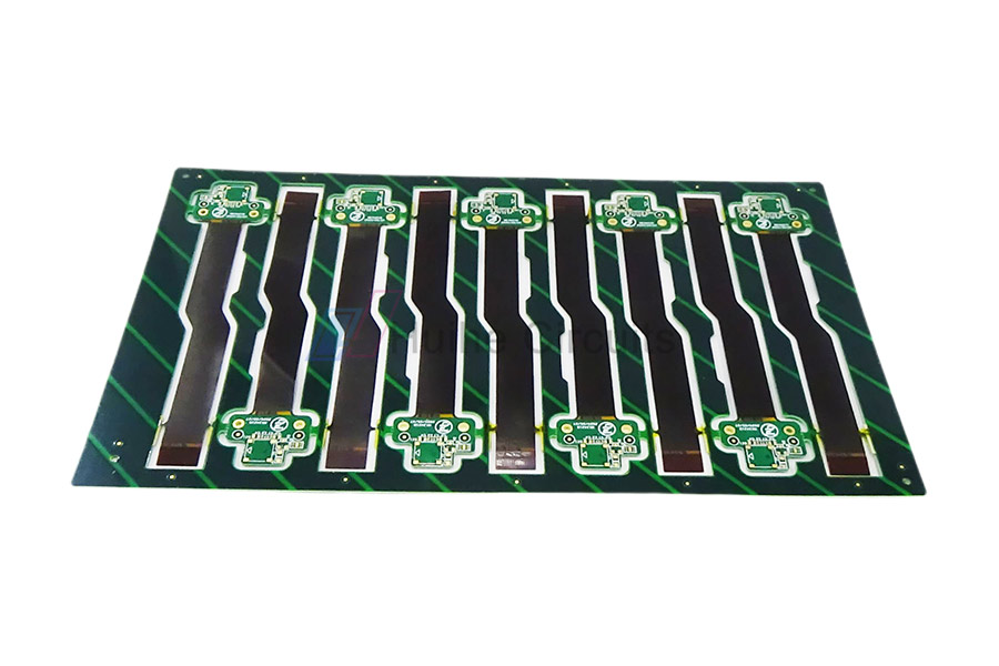
Via In Pad Fr4 PCB


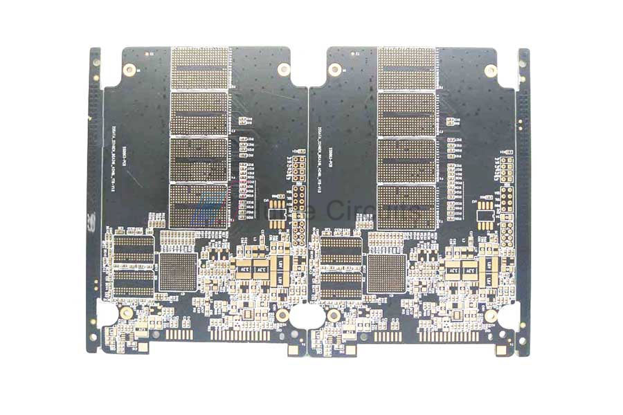
Via In Pad fr4 pcb board, using copper plating or epoxy to fill holesfor circuit board factor, prevent solder paste or flux from flowing into the via in pad, avoid solder ball getting into via or solder mask cover on pad and cause false soldering. HUIHE CIRCUITS Via In PadPCBhas passed ISO9001/ISO13485/IATF16949/UL/RoHS/REACH certification.
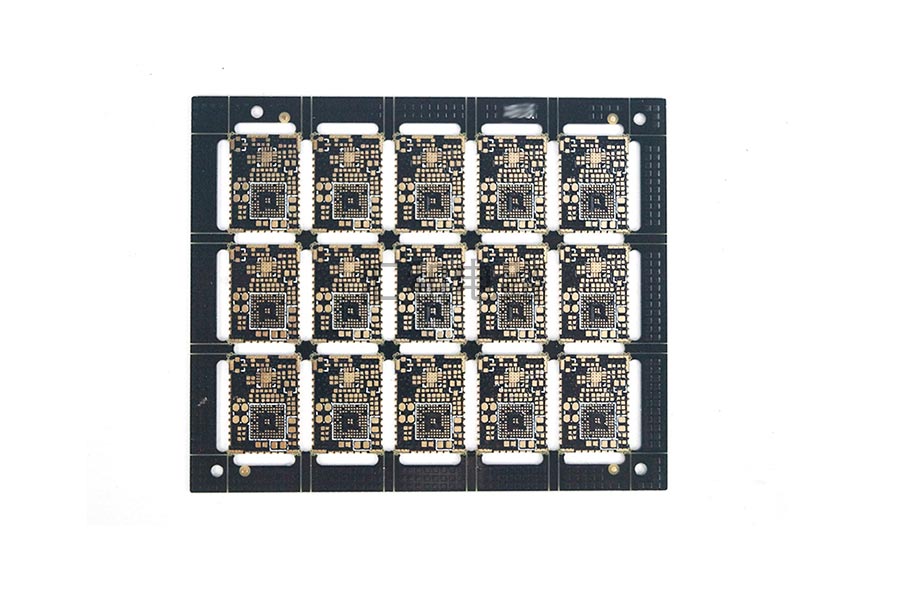
Via In Pad Fr4 PCB List
10 Layer Impedance Control Resin Plugging PCB
16 Layer ENIG Press Fit Hole PCB
6 Layer ENIG via-in-pad Prototype PCB Board
6 Layer ENIG via-in-pad PCB Prototype Service
6 Layer ENIG via-in-pad PCB
8 Layer ENIG via-in-pad PCB
What Is A Hole-In-The-Panel Circuit Board?
The hole in the disk is an important part of the multi-layer PCBChina. It is not only responsible for the main functions of the PCB, but also the cost of drilling usually accounts for 30% to 40% of the fr4 circuit board manufacturingcost. In short, the holes pressed on the pads on the PCB can all be called holes in the disk.
Processing Requirements For Hole Plugs In The Disk
No solder mask ink entering the hole
There should be no tin beads hidden in the hole
No explosive oil, ink pads, making it difficult to mount components, etc.
Common Sense Of PCBCircuitBoard Plug Hole
Prevent the tin from penetrating the component surface from the via hole to cause a short circuit when the PCB is wave soldered
Avoid flux residue in the vias
Prevent the tin balls from popping up during wave soldering, causing short circuits
Prevent surface solder paste from flowing into the hole, causing false soldering and affecting placement
If you want to know more about pcb board material fr4and fr4 pcb thickness, please contact us.
Отправить запрос, связаться с поставщиком
Другие товары поставщика
 |
4 Layer ENIG Impedance Control Half Hole Fr4 PCB | Advantages of cheap 4 layer pcb Own lamination process to convenient production for Multilayer PCB and shorten the lead time. Jiangxi facility is... |
 |
PCB Application | PCB Application As a leading PCB supplier in China printed circuit board industryincluding communications, computers, industrial control, power ... |
 |
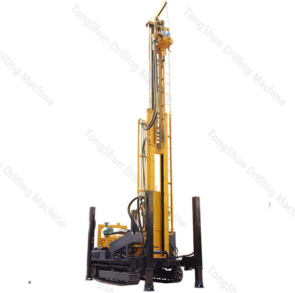
New Energy PCB | Huihe Circuits is your ideal partner, providing you with electromechanical, green energy, renewable energy, PCB manufacturing services and solar la... |
 |
Smart Robot PCB | Smart Robot PCB There are various types of electronic circuit designs for intelligent robots, and various types of PCBs are required.As a pcb co... |
 |
Consumer PCB | The size, thickness and weight of products in the consumer electronics field have been greatly reduced. Via in pad PCB, blind buried vias PCB, half... |