

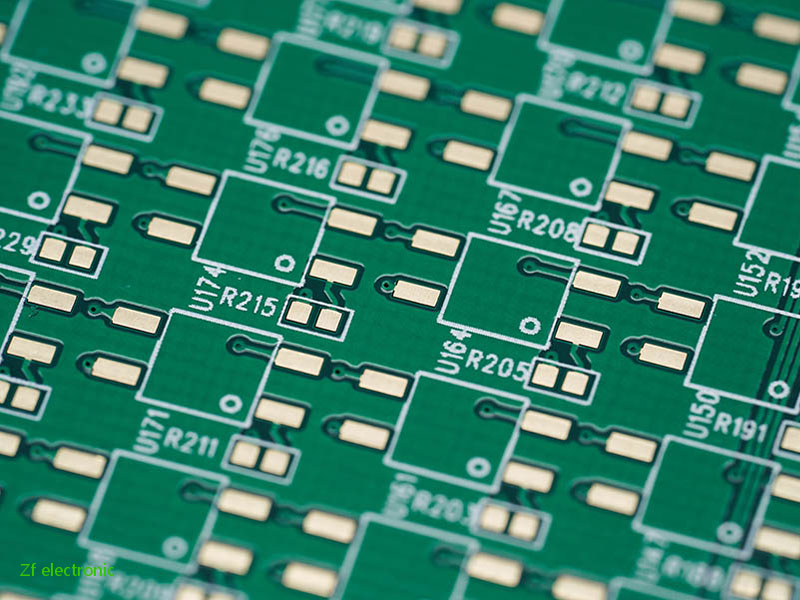
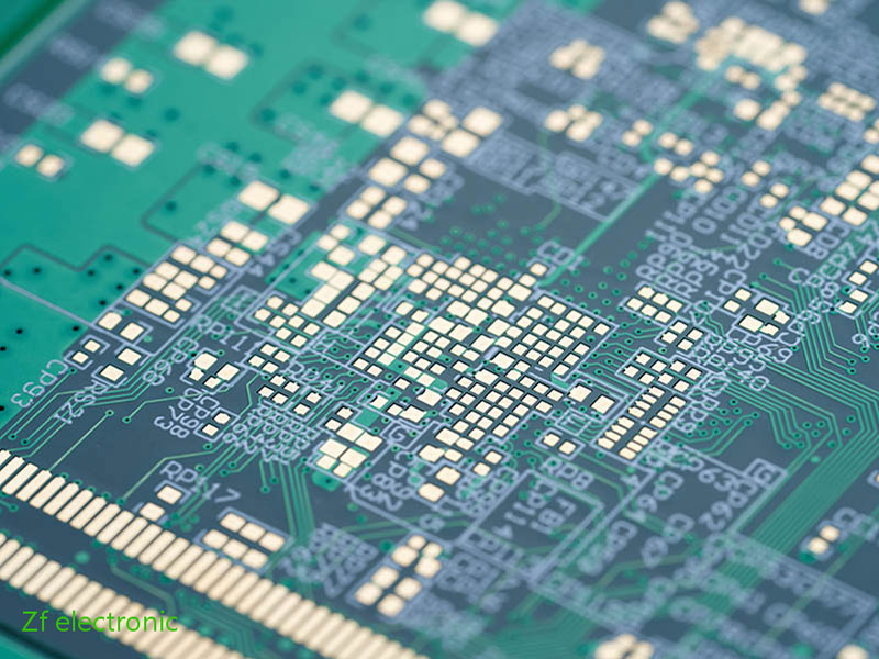
4 Layer PCB


ZF Electronics was founded in 2003, headquartered in Shenzhen China, the world's most complete electronic supply chain. ZF electronics has been one of theprofessional pcb manufacturing companies, from prototype to mass production. Our process includes recommending customers to select easy-to-purchase p/n components in the design stage of a new project and purchasing all electronic components, PCB manufacture, PCBmanufacturing assembly, testing, and fast delivery to our customers.
4 layer PCB boardis laminated on the basis of double-sided PCB, PP and copper foil are added on both sides of the double-sided PCB. Usually, the layout of the4 layer PCB is signal wire-ground wire-power supply-signal.
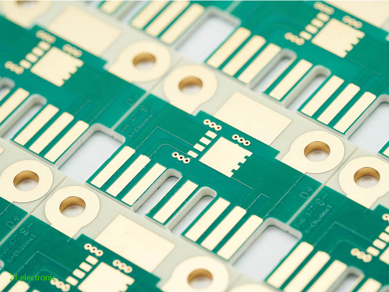
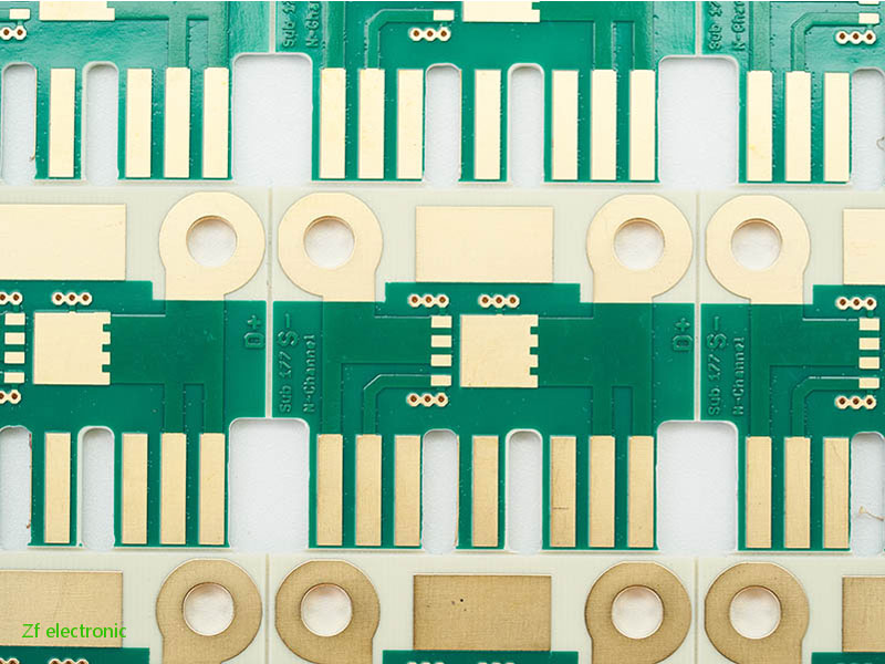
Production of 4 layer PCB
Cheap 4 layer PCBis made by lamination on the basis of the double sided PCB. During the lamination, copper foil and PP are added to the two sides of the double-sided PCB, and then the 4 layer flex PCBis formed by high-temperature pressing. Some people would ask: what is the difference between double sided PCB and four layer PCB? The cropped double sided PCB can be drilled directly on the machine without lamination, while the 4 layer PCB will enter the lamination process after some circuits are etched in the inner layer. Finally, drill holes can be made after lamination.
What are the common rules for designing a 4 layer PCB?
(1) Line width:
Usually, the signal line is set up 6mil, and the remaining power lines are 5V and 3.3V or it can be set up 10mil, 20mil respectively.
(2) Vias:
Normally, there are about 2-3 types of vias on aPCB product. The designed conductor width and conductor spacing should take the production process capability of the 4 layer pcb manufacturerinto consideration. If the conductor width and conductor spacing we designed are over the production capacity of the partner, it may increase unnecessary production costs, and even need to change the supplier. Therefore, when designing the conductor width and conductor spacing, we should basically control it at 4/4mil and the via 12mil, then thePCB 4 layer boardsupplierabove 85% are able to put them into production. The conductor width and conductor spacing here refer to the size between elements such as line-to-hole, line-to-line, line-to-pad, line-to-via when setting rules.
The setting rules consider the design bottleneck in the design file. If there is a 1mm BGA chip, its pin depth is relatively shallow, and only one signal line is needed to be set between two rows of pins and it can be set to 6/6mil. If pin depth is relatively deep, two signal lines need to be taken between the two rows of pins and it can set to 4/4mil. If there is a 0.65mm BGA chip, it needs to be changed to HDI blind via design. Generally speaking, if it is larger than the design bottleneck, then the regional rules can be set. Local line width and moment are designed to be smaller and the other places on the board could be larger to facilitate production and improve the qualification rate.
(3) Copper foil:
Under normal circumstances, modifications can be made.
If you have questions about our 4-layer PCB production capacity, or the specifications required for your custom project are not listed on this page, please feel free to contact us. We will reply within one workday. We will continue to provide quotation support and design support. Welcome to learn about our production process.
Other PCB Fab
Related Videos
Leave a Message
PCB Market
Related News
FAQs
How to Get a Quotation for PCBA (Assembly PCB)?
Please send BOM(Bill of Material/Components) and above mentioned PCB files. It’sbetter if you could supply finished production photos and full requirement detail images.
What will need for PCB clone service?
Please send us the printed circuit board concerned,and also the sharp photos of its front side and the back side.
If you want to know 4 layer pcb price, please contact us.
Отправить запрос, связаться с поставщиком
Другие товары поставщика
 |
Rogers PCB | ZF Electronics, as one of the top rogers pcb manufacturersin China, can provide customers with single-sided PCB, double-sided FR4 PCB, metal core P... |
 |
Plating Through Hole PCB | Plant through hole via PCB or PTH PCB is the most common type. You only need to pick up the PCB to face the light, and the hole that can see the li... |
 |
Metal Core PCB | Metal core PCBchina(printed circuit board), also known as MCPCB board, insulated metal substrate (IMS) or heat dissipation PCBS, is one of the most... |
 |
Multilayer PCB | ZF Electronics, as one of the top pcb fabrication companiesin China, can provide customers with single-sided PCB, double-sided FR4 PCB, metal core ... |
 |
Rogers PCB | With the development of electronics, the production of electronic products also requires more and more materials, such as high-frequency materials.... |
Похожие товары
 |
C500-1.7 Series High Flow Multi-Stage Centrifugal Blower /Centrifugal Blower | Продавец: Greentech International (Zhangqiu) Co., Ltd | Greentech International (Zhangqiu) Co., Ltdis the professional blower supplier.Multistage Centrif... |
 |
Common Rail injector control valve F00VC01303 | Продавец: China Lutong Part Plant | Common Rail injector control valve F00VC01303 Tina#Stainless Steel Cylindrical Pin##Denso Common... |
 |
Common Rail injector control valve F00VC01200 | Продавец: China Lutong Part Plant | Common Rail injector control valve F00VC01200 Tina#Stainless Steel Cylindrical Pin##Denso Common... |
 |
Injector Control Valve Plate 24# | Продавец: China Lutong Part Plant | Injector Control Valve Plate 24# Tina#Stainless Steel Cylindrical Pin##Denso Common Rail Injecto... |
 |
Injector Control Valve Plate 12# | Продавец: China Lutong Part Plant | Injector Control Valve Plate 12# Tina#Stainless Steel Cylindrical Pin##Denso Common Rail Injecto... |
