

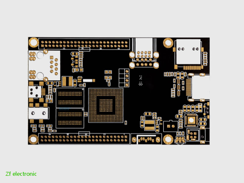
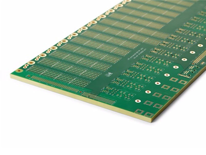
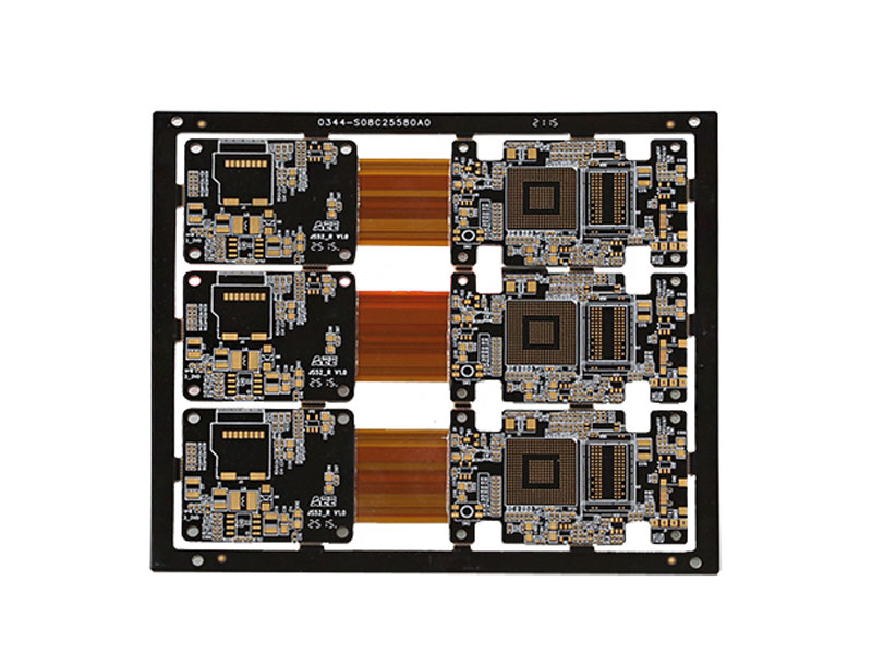
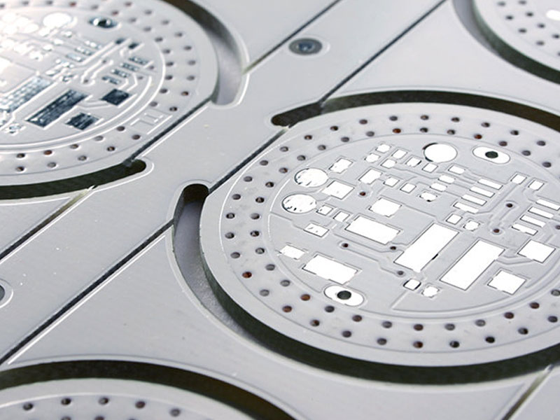
Buried Via PCB


ZF Electronics is a China Shenzhen-based printed circuit board assembly manufacturerand PCB assembler. Shenzhen has been the world's center of electronics R&D and manufacturing for decades. By skipping all the middle pcb manufacturing companies, we are successfully passing the savings and bringing a total satisfaction of PCB/PCBA purchasing experience to our valued customers. That is why 100% of our regular customers come to us for their future orders.
A buried viais a connection of any circuit layer inside the PCB but not connected to the outer layer. The via cannot be drilled after bonding because it must be drilled on the individual circuit layers first. After partially bonding the inner layer, it has to be plated before finishing the bonding, which is more laborious and therefore more expensive than the original through via and blind via. Usually, it is only used in high-density(HDI) PCB to increase the available space for other circuit layers.
The via is an important factor in the design of multi-layer PCB and consists of three main parts, including drill hole, the pad around the hole and the POWER layer. When talking about its process, it should be firstly plated a layer of metal by chemical deposition on the cylindrical surface of the via wall to connect the copper foils that need to be connected to the middle layers. The upper and lower sides of the via will be made into a common pad shape, which can be directly connected with the lines near the two sides or not.
In terms of function, vias can be divided into two categories. One is used for electrical connection between layers while the other is used for fixing or positioning devices. As for the process, the vias can be generally divided into blind via, buried via and through via.
(1) Blind via
Blind via holeis located on the top and bottom surfaces of the PCB with a certain depth. It is used to connect the line on the surface and the underlying inner line and its depth usually does not exceed a certain ratio (aperture).
(2) Buried via
It refers to the connection via that is in the inner layer of buried via PCBwhich will not extend to the surface of the circuit board.
Both of above-mentioned two types of vias are located in the inner layers of the circuit board, which are completed by using a through-via forming process before lamination. There may also be several inner layers overlapping during the via formation process.
(3) Through via
Thethrough hole viaspenetrate the entire circuit board and can be used for internal interconnection or as a positioning via of component installation. Because of its easier implementation and lower cost in the process, most of the PCBs use it instead of the other two kinds of vias.
The advantages of the blind via and buried via
In the non-through-via technology, the application of blind via and buried via can greatly reduce the size and weight, as well as the number of layers and costs inprinting circuit boards, moreover, improve the electromagnetic compatibility, increase the characteristics of electronic products, making the design simpler and faster.
As for the traditional PCB design and processing, there are many problems brought by through vias. First of all, through-vias occupy a large amount of effective space. Secondly, a lot of through-vias densely packed in one place also make the wiring of the inner layers in the multilayer PCB difficult. That is because they will take up the space required for alignment, destroy the impedance characteristics of the power supply and make the power ground plane ineffective. What's worse, the conventional mechanical method of drilling will be 20 times the workload of non-through hole technology.
If you have questions about our buried via PCB production capacity, or the specifications required for your custom project are not listed on this page, please feel free to contact us. We will reply within one workday. We will continue to provide quotation support and design support. Welcome to learn about our production process.
Other PCB Fab
Related Videos
Leave a Message
PCB Market
Related News
FAQs
How to Get a Quotation for PCBA (Assembly PCB)?
Please send BOM(Bill of Material/Components) and above mentioned PCB files. It’s better if you could supply finished production photos and full requirement detail images.
What will need for PCB clone service?
Please send us the printed circuit board concerned,and also the sharp photos of its front side and the back side.
Отправить запрос, связаться с поставщиком
Другие товары поставщика
 |
Thick Copper PCB | PCBs are usually bonded to a layer of copper foil on a glass epoxy substrate, the thickness of which is usually 18μm, 35μm, 55μm and 70&mu... |
 |
Rigid-Flex PCB | ZF Electronics, as one of the top circuit board supplierin China, can provide customers with single-sided PCB, double-sided FR4 PCB, metal core PCB... |
 |
Rigid PCB | PCB can be divided into rigid PCB and flexible PCB according to the production materials. The rigid PC boardcontains phenolic paper laminate, epoxy... |
 |
Aluminum PCB | ZF Electronics was founded in 2003, headquartered in Shenzhen China, the world's most complete electronic supply chain. ZF electronics has been one... |
 |
Plating Through Hole PCB | Plant through hole via PCB or PTH PCB is the most common type. You only need to pick up the PCB to face the light, and the hole that can see the li... |
Похожие товары
 |
C500-1.7 Series High Flow Multi-Stage Centrifugal Blower /Centrifugal Blower | Продавец: Greentech International (Zhangqiu) Co., Ltd | Greentech International (Zhangqiu) Co., Ltdis the professional blower supplier.Multistage Centrif... |
 |
Common Rail injector control valve F00VC01303 | Продавец: China Lutong Part Plant | Common Rail injector control valve F00VC01303 Tina#Stainless Steel Cylindrical Pin##Denso Common... |
 |
Common Rail injector control valve F00VC01200 | Продавец: China Lutong Part Plant | Common Rail injector control valve F00VC01200 Tina#Stainless Steel Cylindrical Pin##Denso Common... |
 |
Injector Control Valve Plate 24# | Продавец: China Lutong Part Plant | Injector Control Valve Plate 24# Tina#Stainless Steel Cylindrical Pin##Denso Common Rail Injecto... |
 |
Injector Control Valve Plate 12# | Продавец: China Lutong Part Plant | Injector Control Valve Plate 12# Tina#Stainless Steel Cylindrical Pin##Denso Common Rail Injecto... |
