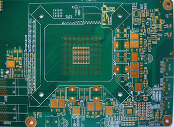
HDI PCB, High Density Interconnect PCB, HDI PCB Manufacturing


High Density Interconnects (HDI) are used to meet the market demand
for complex designs in smaller form factors across the majority of
market segments, (Wireless, Telecom, Military, Medical, Semiconductor,
and Instrumentation).HDI Circuit boards, one of the fastest growing technologies in PCBs, HDI
Boards contain blind and/or buried vias and often contain microvias of
.006 or less in diameter.They have finer lines and spaces always = <3mil They have a higher circuitry density than traditional circuit boards.MOKO maintains years of experience with HDI products and was a
pioneer of second generation microvias. now offer an entire family of
microvia technology solutions for your next generation products.HDI Board General InformationHigh Density Interconnects (HDI)
board are
defined as a board (PCB) witha higher wiring density per unit area than
conventional printed circuit boards (PCB). They have finer lines and
spaces (<100 µm), smaller vias (<150 µm) and capture pads (<400
µm), I/O>300,
and higher connection pad density (>20 pads/cm2)
than employed in conventional PCB technology. HDI board is used to reduce size and weight, as well as to enhance
electrical performance.According to layer up different, currently DHI board is divided into three basic types:1) HDI PCB (1+N+1)HDI PCB, High Density Interconnect PCB Features: Suitable for BGA with lower I/O counts Fine line, microvia and registration technologies capable of 0.4 mm ball pitch Qualified material and surface treatment for Lead-free process Excellent mounting stability and reliability Copper filled viaHDI PCB, High Density Interconnect PCB Application: Cell , UMPC, MP3 Player, PMP, GPS, Memory Card1+N+1 HDI PCB Structure:2) HDI PCB (2+N+2)HDI PCB, High Density Interconnect PCB Features: Suitable for BGA with smaller ball pitch and higher I/O counts Increase routing density in complicated design Thin board capabilities Lower Dk / Df material enables better signal transmission performance Copper filled viaHDI PCB, High Density Interconnect PCB Application: Cell , PDA, UMPC, Portable game console, DSC, CamcorderHDI PCB CapabilitiesItemCapabilitiesLayers3 - 50 LayersHDI Step3+N+3Min.Line Width0.05mm (2 mil)Min.Line Space0.05mm (2 mil)Min.Annular ring0.1mm (4 mil)Min. Via0.1mm (4 mil)Max.Size500mm X 800mmMaterialFR4,High Tg220Material thicknessStart at 25um Plus copperCopper thickness0.3 OZ to 10 OZ (10um - 350um)Please contact us for more information about HDI PCB Board.
Другие товары поставщика
|
|
|
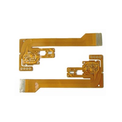
Flex Printed CircuitsFlexible printed circuits were originally designed as a
replacement for traditional wire harnesses. From early applications
... |
|
|
|
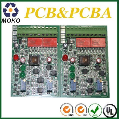
Moko Technology Ltd is one of the leading China assembled led board pcb manufacturers and suppliers with professional assembled led board pcb facto... |
|
|
|
Moko Technology Ltd is one of the leading China power supply pcb circuit board partern manufacturers and suppliers with professional power supply p... |
|
|
|
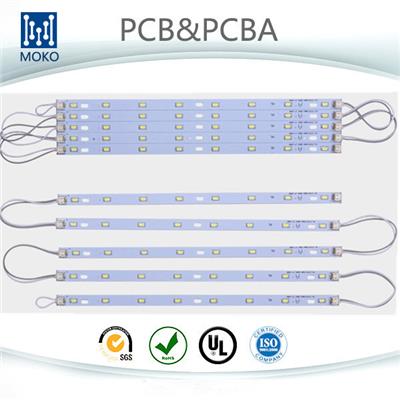
Looking for LED Tube PCB or Find Good Quality LED Light PCB assembly service manufacturers from China? MOKO Specialize in LED Light PCB, LED Tube P... |
|
|
|
MOKO is an ISO 9001:2008 circuits assembly factory of printed circuit boards.We specialize in quickturn prototype manufacturing and assembly, and p... |
Все товары поставщика
Похожие товары