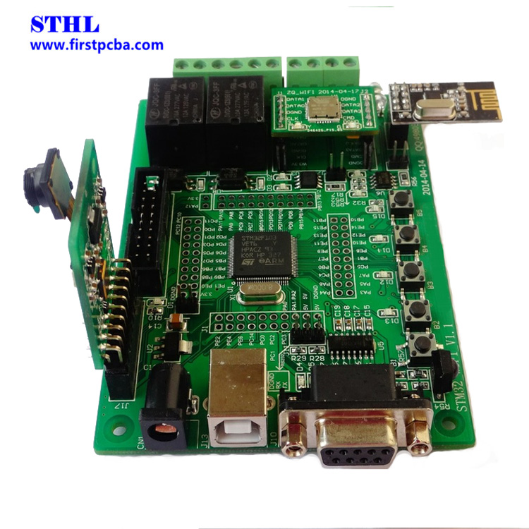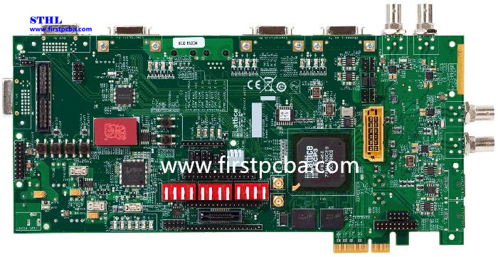
16 Layer ENIG Press Fit Hole PCB

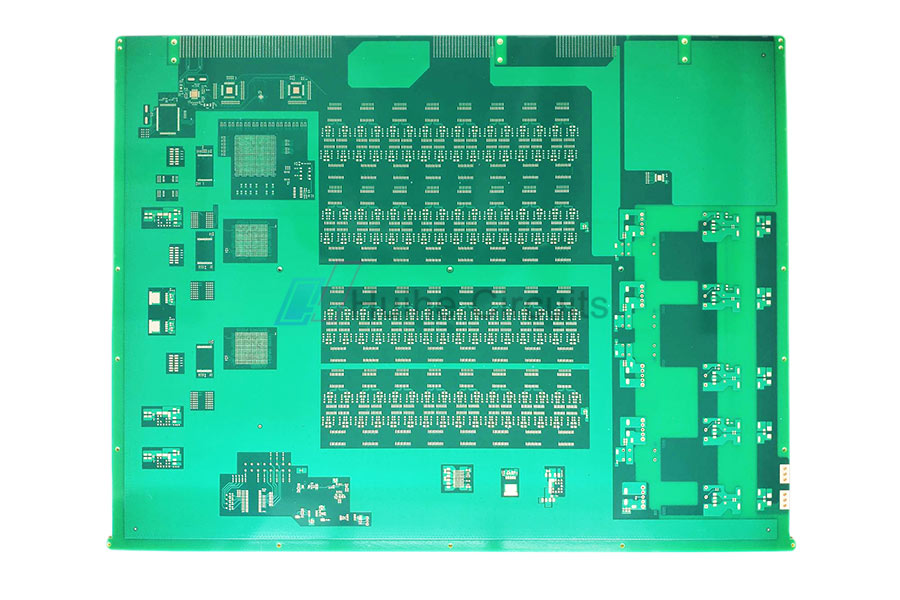
Number of layers: 16
Surface finish: ENIG
Base material: FR4
Thickness: 3.0mm
size:420×560mm
Outer Layer W/S: 4/3mil
Inner layer W/S: 5/4mil
Aspect Ratio: 9:1
Special process: via-in-pad Impedance Control Press Fit Hole
Advantages Of 16 Layer ENIG Press Fit Hole Pth PCB
Own lamination process to convenient production for Multilayer PCB and shorten the lead time.
Jiangxi facility is environmental-friendly approved by the government .
Famous raw materials brand, Kingboard, Shengyi, ITEQ, Taiyo, Guangxin.
Highly automated production line with AIO Optical Scanning, Electroplating Automatic Line, High-speed flying probe test machines and inkjet printer.
Engineers with more than 15 years of experience
Perfect quality inspection system
Professional R&D team can make all kinds of special boards.
Quick turn, prototype, medium or large batches can be produced to meet the needs of different customers.
Sales office in Shenzhen and own 12,000sqm factory in Jiangxi.
Establish an e-commerce system to reduce transaction costs and increase market response speed.
As a 16 layer pcb manufacturer, we can offer types of 16 layer pcbfor sale, if you are interested, please contact us.
There are many printed circuit board manufacturersin China, but we are one of the best choices for sale, if you have needs, please contact us.
If you want to know more different types of pcb board, please visit our website.
Отправить запрос, связаться с поставщиком
Другие товары поставщика
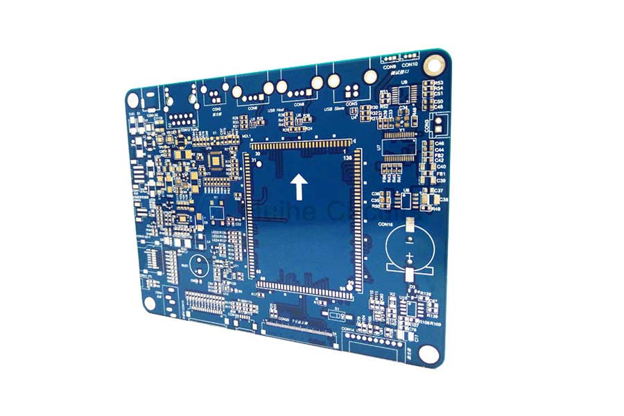 |
Layer HASL Blind Buried Via PCB | Number of layers: 6 Surface finish: HASL Base material: FR4 Outer Layer W/S: 9/4mil Inner layer W/S: 11/7mil Thickness:1.6mm Special process: Blind... |
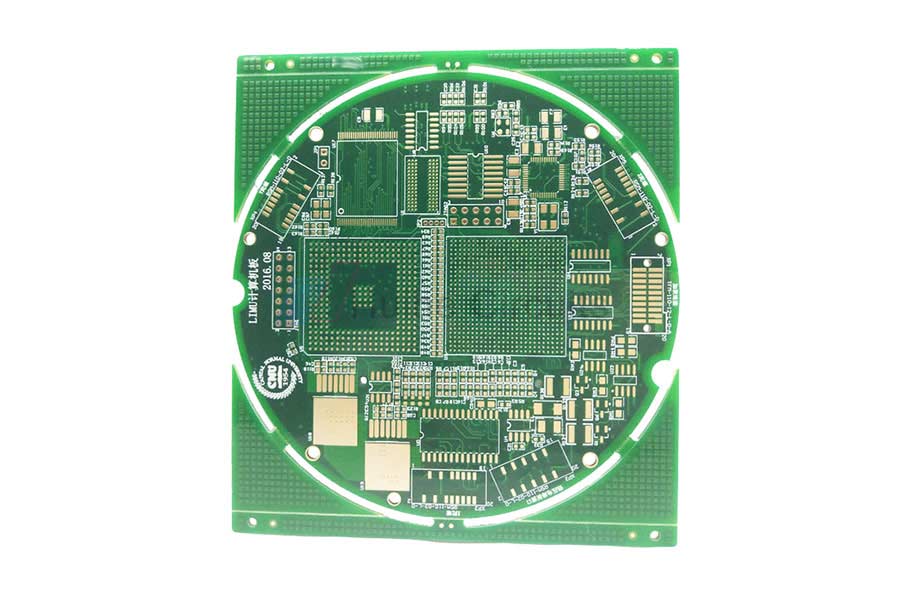 |
Blind Buried Vias & Hdi Pcb | Blind & Buried Via Board, use micro blind vias to increase the trace distribution density. Improve radio frequency, electromagnetic wave interf... |
 |
High Tg PCB | PCB High TG, electric circuit board Glass transition temperature Tg≥170℃, electric pcb circuitboard High heat resistance is suitable for lead-fr... |
 |
6 Layer LF-HASL PCB | Number of layers: 6 Surface finish: LF-HASL Base material: FR4 Outer Layer W/S: 11/6mil Inner layer W/S: 16/5mil Thickness: 1.6mm Advantages ... |
 |
2 Layer OSP Impedance Control Half Hole PCB | Advantages Of 2 Layer OSP Impedance Control Half Hole PCB Own lamination process to convenient production for Multilayer PCB and shorten the lead ... |