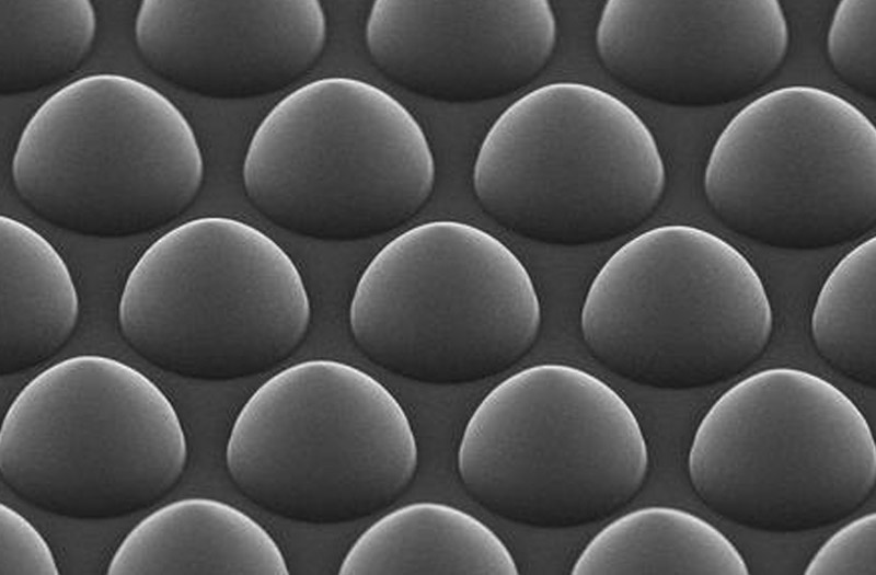
PATTERNED SAPPHIRE SUBSTRATES


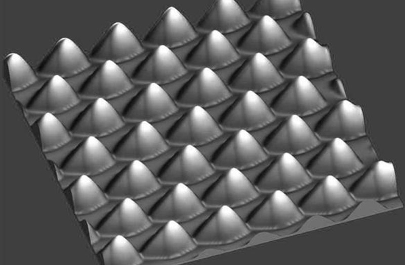
Sapphire wafer is the most widely used substrate material in semiconductor lighting industry, and pattern sapphire substrate(PSS) is the general method to improve the luminous efficiency of semiconductor lighting devices. These sapphire substrates are with periodic structures of various shapes such as cone, dome, pyramid, and pillar, etc.
Cryscore's Excellent Patterned Sapphire Substrates
Pattern dimension, aspect ratio, and uniformity across the wafer as well as consistency from wafer to wafer, are important factors to improve the light extraction. Currently, we provide 2-inch and 4-inch patterned optical sapphiresubstrates (pss waferand pss sapphire) with the following specifications. Diameter: 2.7 +/- 0.1 μm. Spacing: 0.3 +/- 0.1 μm. Depth: 1.7 +/- 0.15 μm.
Send product request
Other supplier products
 |
PATTERNED SAPPHIRE SUBSTRATES | Sapphire wafer is the most widely used substrate material in semiconductor lighting industry, and patterned sapphire substrate(PSS) is the general ... |
 |
A-PLANE (11-20) SAPPHIRE WAFERS | A plane sapphirewafers have a uniform dielectric constant and highly insulating characteristic, so they are generally used for hybrid microelectron... |
 |
GaN on Sapphire | As a professional sapphire wafermanufacturer, CRYSCORE can provide standard or optical sapphirewafers with any orientation applied to epitaxy, as w... |
 |
CUSTOM SAPPHIRE WINDOWS | Due to the extensive applications of sapphire in various fields, different dimensions are required. CRYSCORE can provide custom sapphire windowswit... |
 |
CUSTOM SAPPHIRE WAFERS | CRYSCORE supplies sapphire wafers with the high-quality surfaces in all orientations (C-planesapphire, A plane sapphire, R-planesapphire, M plane s... |
Same products
 |
Micronized polypropylene wax for injection moulding | Seller: Syntop chemical Co.,Ltd. | The incorporation of polypropylene micronized wax into injection moulding processes delivers the ... |
 |
Drum Type Mobile Mixing Station | Seller: Yousheng Machinery Equipment Co.,Ltd | Drum Type Mobile Mixing Station Drum Type Mobile Mixing StationPortable Drum Concrete Batch Plan... |
 |
Washable Cheap 13.56Mhz 213 Nfc Mini Stickers 13.56 Mhz RFID Label Sticker Tag HF/UHF Tags Dry Inlay | Seller: XIUCHENG RFID | Size:On request Material:PET, PVC,paper or customized Frequency:UHF/HF Printing:Thermal transf... |
 |
Micronized wax used for industrial paint processing | Seller: Syntop chemical Co.,Ltd. | Micronized wax is a vital functional additive in industrial paint processing, with primary functi... |
 |
Plant Growth Regulator Manufacturer | Seller: HEBEI LAIKE BIOTECH CO.LTD | Plant Growth Regulator Manufacturer Plant Growth Regulator Manufacturer - Laike Biotech spec... |