

PATTERNED SAPPHIRE SUBSTRATES


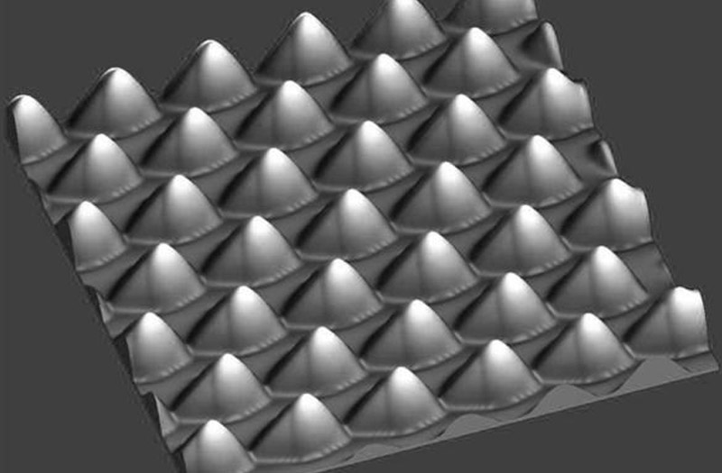
Sapphire wafer is the most widely used substrate material in semiconductor lighting industry, and pattern sapphire substrate(PSS) is the general method to improve the luminous efficiency of semiconductor lighting devices. These sapphire substrates are with periodic structures of various shapes such as cone, dome, pyramid, and pillar, etc.
Cryscore's Excellent Patterned Sapphire Substrates
Pattern dimension, aspect ratio, and uniformity across the wafer as well as consistency from wafer to wafer, are important factors to improve the light extraction. Currently, we provide 2-inch and 4-inch patterned optical sapphiresubstrates (pss waferand pss sapphire) with the following specifications. Diameter: 2.7 +/- 0.1 μm. Spacing: 0.3 +/- 0.1 μm. Depth: 1.7 +/- 0.15 μm.
在线联系供应商
Other supplier products
 |
SAPPHIRE WAFERS / SAPPHIRE SUBSTRATES | Due to the less mismatched lattice and stable chemical and physical properties, sapphire(Al2O3) wafer is the popular substrates for III-V nitrides,... |
 |
CUSTOM SAPPHIRE WINDOWS | Due to the extensive applications of sapphire in various fields, different dimensions are required. CRYSCORE can provide custom sapphire windowswit... |
 |
M-PLANE (10-10) SAPPHIRE WAFERS | Due to its application prospects in solar-blind ultraviolet detection, MgZnO alloy semiconductor films with suitable band gaps have attracted more ... |
 |
SAPPHIRE INGOTS/RODS | Sapphire ingotsare typically used as raw materials for further processing. These sapphire rods and sapphire ingots are uniformly shaped, usually as... |
 |
SAPPHIRE INGOTS/RODS | SAPPHIRE INGOTS/RODS Sapphire ingots are typically used as raw materials for further processing. These sapphire rod and sapphire ingots are uniform... |
Same products
 |
C500-1.7 Series High Flow Multi-Stage Centrifugal Blower /Centrifugal Blower | 卖方: Greentech International (Zhangqiu) Co., Ltd | Greentech International (Zhangqiu) Co., Ltdis the professional blower supplier.Multistage Centrif... |
 |
Common Rail injector control valve F00VC01303 | 卖方: China Lutong Part Plant | Common Rail injector control valve F00VC01303 Tina#Stainless Steel Cylindrical Pin##Denso Common... |
 |
Common Rail injector control valve F00VC01200 | 卖方: China Lutong Part Plant | Common Rail injector control valve F00VC01200 Tina#Stainless Steel Cylindrical Pin##Denso Common... |
 |
Injector Control Valve Plate 24# | 卖方: China Lutong Part Plant | Injector Control Valve Plate 24# Tina#Stainless Steel Cylindrical Pin##Denso Common Rail Injecto... |
 |
Injector Control Valve Plate 12# | 卖方: China Lutong Part Plant | Injector Control Valve Plate 12# Tina#Stainless Steel Cylindrical Pin##Denso Common Rail Injecto... |
