Silicon Epitaxial Wafer
Epitaxy is the process of depositing a thin layer on substrate, Epitaxy layer can be as the same as the basis(Si/Si) or different with the basis (SiGe/Si or SiC/S) ,Silicon epitaxy is a layer of single-crystal silicon on wafer,The epitaxial layer can be doped, as it is deposited, to the precise doping concentration while continuing the substrate's crystalline structure. We can offer Silicon epitaxial wafer and SiGe Epitaxial Wafer,diameter from 4” to 8” . Wafer Type: Blanket Epitaxial Wafer, Patterned Epitaxial Wafer with Burried Layer. Application: Bipolar device, Power MOSFET,IGBT,Detectors and rectifier, IC and As-doped substrate.
Other supplier products
|
|
SiC(Silicon Carbide)Wafer |
PWAM offers semiconductor materials,SiC substate for GaN epitaxy device,power devices, high-temperature device and optoelectron
PWAM offers semic... |
|
|
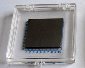
CZT Wafer |
CdZnTe (Cadmium Zinc Telluride,CZT) is a new semiconductor, which enables to convert radiation to electron effectively, it is mainly used in infrar... |
|
|
GaAs (Gallium Arsenide) Wafers |
PWAM Develops and manufactures compound semiconductor substrates-gallium arsenide crystal and wafer.We has used advanced crystal growth technology,... |
|
|
Silicon Epitaxial Wafer |
Epitaxy is the process of depositing a thin layer on substrate, Epitaxy layer can be as the same as the basis(Si/Si) or different with the basis (S... |
|
|
Semiconductor wafer |
|
供应产品
Same products