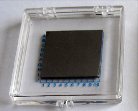
CZT Wafer
CdZnTe (Cadmium Zinc Telluride,CZT) is a new semiconductor, which enables to convert radiation to electron effectively, it is mainly used in infrared thin-film epitaxy substrate, nuclear radiation detection,X-ray and γ-ray detection, laser optical modulation, high-performance solar cells and other high-tech fields.
From 2001,PWAM offers commercial CZT wafers with high quality and very competitive price. We also can offer CZT crystals with contacts. Regulaly contacts of anodes and cathode are both deposited by Au, but we can use Al to the deposit the contacts as required.And we offer wafer custom size.
Other supplier products
|
|
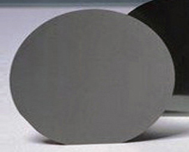
Ge(Germanium)Wafer |
Germanium blank or window are used in night vision and thermographic imaging solutions for commercial security, fire fighting and industrial monito... |
|
|
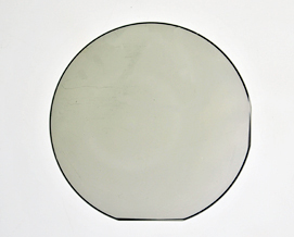
Silicon Epitaxial Wafer |
Epitaxy is the process of depositing a thin layer on substrate, Epitaxy layer can be as the same as the basis(Si/Si) or different with the basis (S... |
|
|
SiC(Silicon Carbide)Wafer |
PWAM offers semiconductor materials,SiC substate for GaN epitaxy device,power devices, high-temperature device and optoelectron
PWAM offers semic... |
|
|
CZT Wafer |
CdZnTe (Cadmium Zinc Telluride,CZT) is a new semiconductor, which enables to convert radiation to electron effectively, it is mainly used in infrar... |
|
|
Semiconductor wafer |
|
All supplier products
Same products
|
|
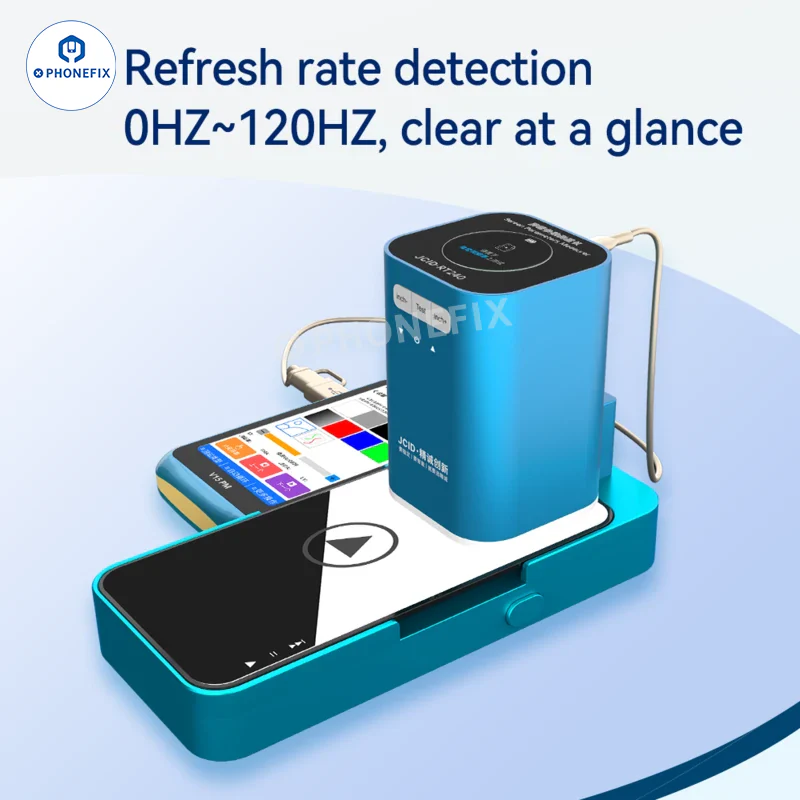
JCID RT240 Screen Resolution Refresh Rate Parameters Measurer |
Seller: PHONEFIX technology Co.,Ltd |
JCID RT240 Screen Parameters Measurer for Mobile Phone/iPhone Display Resolution and Refresh Rate... |
|
|
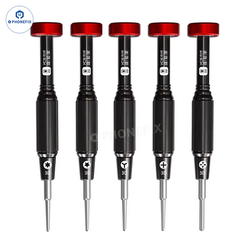
IKS-T05 ZD Skrevdrever Network 5-In-1 Magnetic Bits Disassembly Tool |
Seller: PHONEFIX technology Co.,Ltd |
YCS-T05 5-in-1 3D Screwdriver set with 5 pieces magnetic extra-hard bit for assembling/disassembl... |
|
|
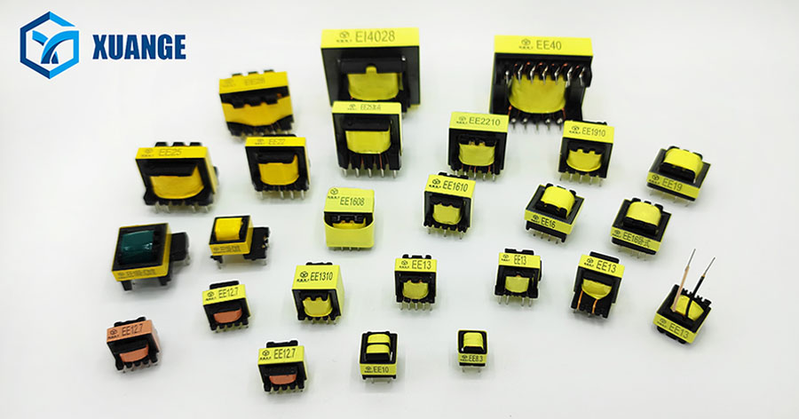
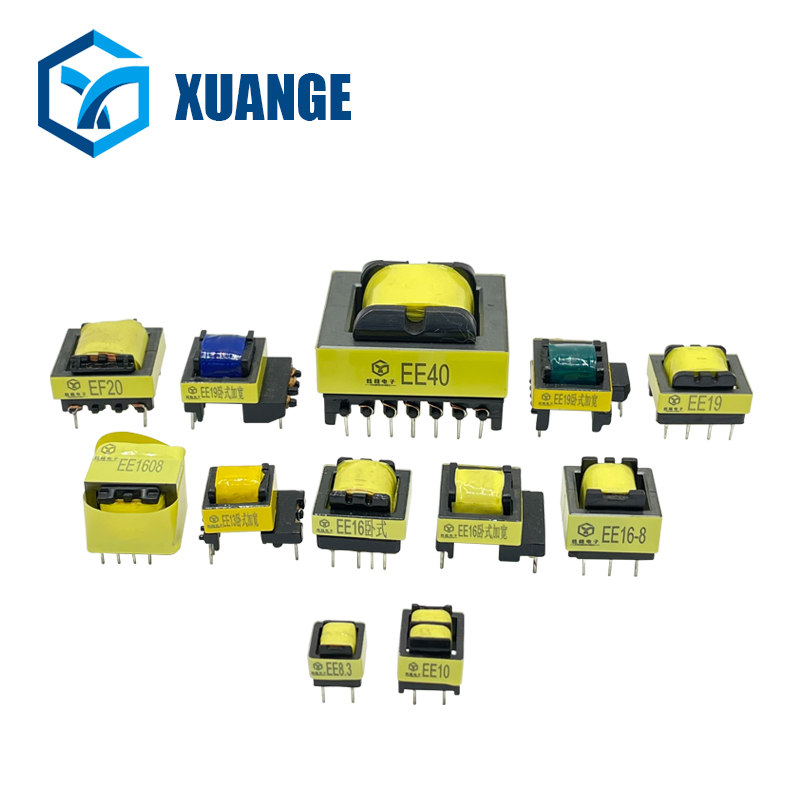
ee8.3-ee60 transformer | transformer manufacturers |
Seller: XuanGe Electronics Manufacturer |
EE model:EE8.3, EE10/11, EE13, EE16, EEL16, EE19, EE20, EE22, EE25, EE25.4, EE30, EE35, EE40, EE4... |
|
|
ee8.3-ee60 transformer | transformer manufacturers |
Seller: XuanGe Electronics Manufacturer |
EE model:EE8.3, EE10/11, EE13, EE16, EEL16, EE19, EE20, EE22, EE25, EE25.4, EE30, EE35, EE40, EE4... |
|
|
Cisco Catalyst WS-C3850-12S-S Layer 3 Switch |
Seller: 840499 |
Features: Auto-negotiation, ARP support, trunking, VLAN support, auto-uplink (auto MDI/MDI-X), IG... |