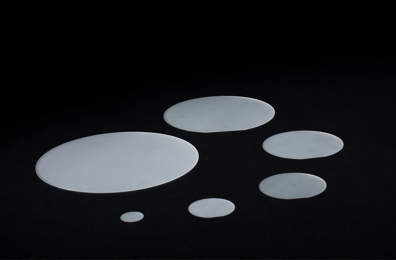
PATTERNED SAPPHIRE SUBSTRATES
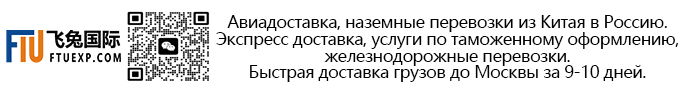

Sapphire wafer is the most widely used substrate material in semiconductor lighting industry, and patterned sapphire substrate(PSS) is the general method to improve the luminous efficiency of semiconductor lighting devices. These sapphire substrates are with periodic structures of various shapes such as cone, dome, pyramid, and pillar, etc.
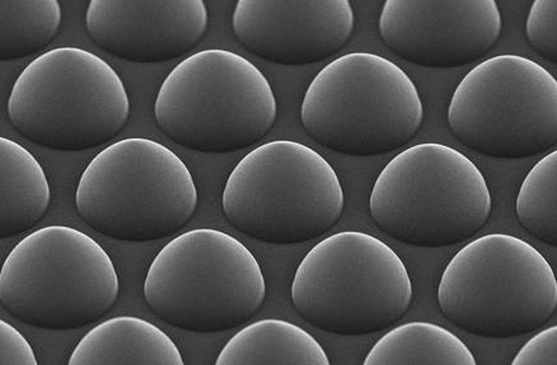
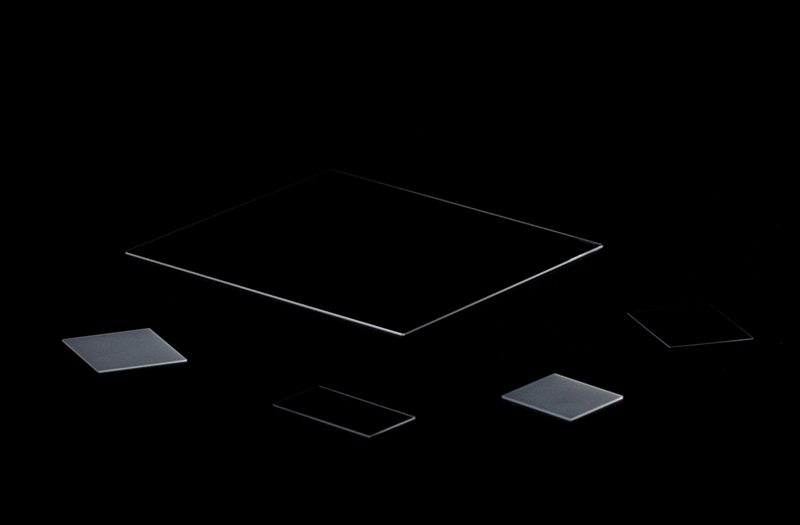
Different Sizes of Patterned Sapphire Substrates
2-Inch
2 Inch Patterned Sapphire Substrates
PSS is to design and manufacture specific nano-scale microstructure pattern on sapphire substrate.
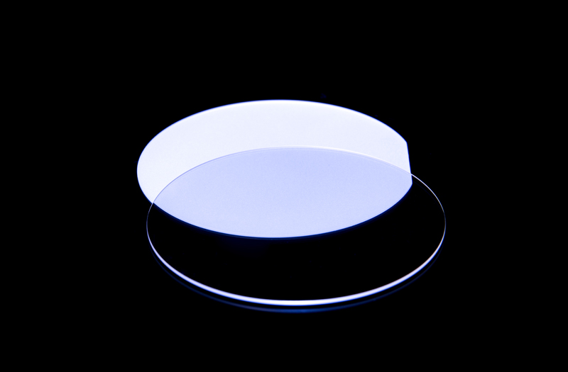
4-Inch
4 Inch Patterned Sapphire Substrates
Patterned Sapphire Substrates (PSS) is micro-patterned sapphire substrate used to for GaN based light emitting diodes(LEDS).
CRYSCORE OPTOELECTRONIC LIMITED has been a professional manufacturer, we provide sapphire optics, pss wafer, pss sapphire, Patterned sapphire substrateand etc. Want to know more? Please contact us.
Отправить запрос, связаться с поставщиком
Другие товары поставщика
 |
4 INCH C-PLANE(0001) SAPPHIRE WAFERS | Wafer saphiris being used extensively as a substrate for III-V nitrides and for many other epitaxial films. We supply 99.999% high purity sapphire ... |
 |
SAPPHIRE WINDOWS | SAPPHIRE WINDOWS Sapphire has a wide transmission range, spanning the three wavelength bands of ultraviolet, visible light and infrared and has hi... |
 |
CUSTOM SAPPHIRE WAFERS | CUSTOM SAPPHIRE WAFERS CRYSCORE supplies sapphire wafers with the high-quality surfaces in all orientations (C-plane, A-plane, R-plane, sapphire m... |
 |
Silicon on Sapphire | As a professional sapphire wafermanufacturer, CRYSCORE can provide standard or optical sapphirewafers with any orientation applied to epitaxy, as w... |
 |
0391-393 3936 | R-PLANE (1-102) SAPPHIRE WAFERS R plane sapphire wafers are preferred for the hetero-epitaxial deposition of silicon used in microelectronic IC app... |
Похожие товары
 |
Micronized polypropylene wax for injection moulding | Продавец: Syntop chemical Co.,Ltd. | The incorporation of polypropylene micronized wax into injection moulding processes delivers the ... |
 |
Drum Type Mobile Mixing Station | Продавец: Yousheng Machinery Equipment Co.,Ltd | Drum Type Mobile Mixing Station Drum Type Mobile Mixing StationPortable Drum Concrete Batch Plan... |
 |
Washable Cheap 13.56Mhz 213 Nfc Mini Stickers 13.56 Mhz RFID Label Sticker Tag HF/UHF Tags Dry Inlay | Продавец: XIUCHENG RFID | Size:On request Material:PET, PVC,paper or customized Frequency:UHF/HF Printing:Thermal transf... |
 |
Micronized wax used for industrial paint processing | Продавец: Syntop chemical Co.,Ltd. | Micronized wax is a vital functional additive in industrial paint processing, with primary functi... |
 |
Plant Growth Regulator Manufacturer | Продавец: HEBEI LAIKE BIOTECH CO.LTD | Plant Growth Regulator Manufacturer Plant Growth Regulator Manufacturer - Laike Biotech spec... |