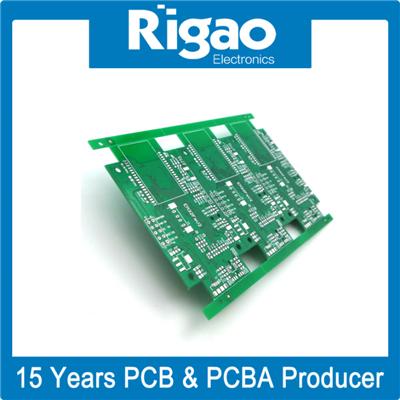
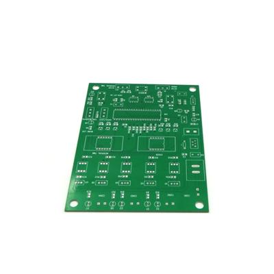
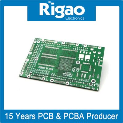
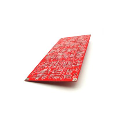
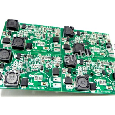
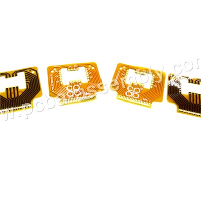
HDI PCB Project, PCB Manufacturer


Among those famous hdi pcb project, pcb manufacturer manufacturers, Rigao Electronics is a professional hdi pcb project, pcb manufacturer supplier and factory, we can offer you customized products price and quotation consultation, welcome to buy our products at low price.Basic Info.Model NO.:pcb-558Type:Rigid Circuit BoardDielectric:FR-4Material:Fiberglass EpoxyApplication:AerospaceFlame Retardant Properties:V0Mechanical Rigid:RigidProcessing Technology:Electrolytic FoilBase Material:CopperInsulation Materials:Epoxy ResinBrand:RigaoPackage:Vacuum Packing with Desiccant, Export CartonSpecification:TS16949, SGS, ISO14000, REACH, RoHSTrademark:Shenzhen Rigao Electronics Co., LtdOrigin:Shenzhen, GuangdongWe Found:in 2008Land Area of Our Factory:More Than 10000 Square MeterBusiness Nature:Manufacturing of Printed Circuit BoardPCB Layers:1~16PCB Surface Finishes:HASL(Lead Free), Enig, OSP, Gold Finger, Tin, etc.PCB Max. Size:1200mm×600mmLaminate Materials:Fr-4,Fr-1,,Fr-2,Cem-1,Cem-3Certificate:RoHS, ISO14000, CE, UL,Production Capacity:100000 Square Meter/MonthProduct DescriptionWelcome to Shenzhen Rigao Electronics Co., LtdWe are the Printed Circuit Boards (PCB) manufacturer with 8 years experience, specialized in single-sided, 2-layerd, multilayer and high density interconnector (HDI) PCB. We take strict Japanese-pattern management, so please trust us with your orders! Certification: UL, ISO14001, ISO9001, SGS, ROHS Our PCBs are used for auto industry, high power led, Office Appliance, electric toy, machinery, industrial lighting and so on. Our Corporate Vision: To become the world's most trustful PCBOur Corporate Values: Excellence, customer satisfaction, innovation and integrity, green.Our Quality Target:1.Ptoduction pass rate>99%2.Timely delivery rate>98%3.Customer complaint rate<1%4.Customer satisfaction rate>99%Environmental Guideline:Protect the environment, prevent pollution, save resources, and reduce waste. PCB Manufacture Quality Control:1. Engineering pretreatment before production2. 100% E-test, 100% visual inspection3. AOI inspection 4. High voltage test, impedance control test5. Micro section, soldering capacity, thermal, shocking test6. Reliability test, insulating resistance test, ionic cleanliness testing Our PCB process capability PCB DescriptionOur PCB Board CapabilityPCB Surface Finisheselectrolytic nickel-gold,HASL(Lead Free, ENIG (Electroless Nickel/Immersion Gold, Carbon Ink, Golden Fingers, OSP (Entek, Immersion Tin, Immersion SilverPCB Max. Size1200mm×600mmPCB Min. Size5mm×5 mmBow & Twist ToleranceSingle Side≤1.0%,Double Side≤0.7%, Muti-Layer≤0.5%Min. Board Thickness & Tolerance0.2mm±0.08mmPCB Min. trace/spacingTin board:0.2mm±20%(8mil±0%)gold board:0.075mm±20%(3mil±0%)Copper to Board Edge Spacing0.5mm(20mil)Hole to Trace Spacing0.3mm(12mil)Min. Hole Diameter0.2mm±.076mm(8mil±3mil)Min. Hole Clearance0.4mm±.076mm(16mil±3mil)Copper Thickness on Hole Wall20-25um(0.79mil-1.0mil)Hole Location Tolerance±0.076mm(l±3mil)Min Diameter of Punching HoleFR-4 board thickness≤1.0mm(40mil):1.0mm(40mil)FR-4 board thickness 1.2-3.0mm(48-120mil):1.5mm(60mil)PCB Min. Punching SlotFR-4 CEM-3 board thickness≤1. 0mm(40mil):0.8 mm×0.8 mm(32mil×32mil)FR-4 board thickness1.2-3.0mm(48-120mil): 1.0 mm×1.0 mm(40mil×40mil)Trace width variation±0.076mm(±3mil)Outline ToleranceRouting:±0.1mm (±4mil) ,Punching:±0.05mm (±2mil)V-CUT Registration Tolerance±0.2mm (±8mil)PCB BOARD TypeSingle-sided, double-sided, multi-layerMajor MaterialFR-4, CEM-1,CEM-3, high frequency laminates, Aluminum, NiFe-based, copper basePCB BOARD Thickness0.2-3.5mmBase Copper Thickness11um 35um 70um 105umMax. aspect ratio(board thickness: hole size)8:1V-Cut Angle Tolerance±5°V-Cut Board Thickness0.4mm -3.2mm(16mil -128mil)Min SMT Pitch0.3mm(12mil)Min. Component mark0.15mm(6mil)Min. width of annular ring(finished)0.15mm(6mil)/sideMin pad opening0.076mm(3mil)Min S/M Bridge±0.076mm(±3mil)carbon ink board manufacturing capability:1.Impedance Control:20K±10% 2.Hardness:6H 3.bearable friction times :above 200000 timesWhat we need:Please tell us the information as below: NO.ItemsNO.Items1Board for what product8Surface Finish2Number of Layers9Board Material3Copper Thickness(um)10Board Thickness(um)4Solder Mask Color11PCB Dimensions(mm)5Silk Screen Color12Min Finished Hole Size(mm)6Milling13Min Clearance(mm)7Min Track Width(mm)14Other special requirementsPCB Fast delivery: PackagingVacuum Packing with desiccant,Professional Export Carton.Deliverytime Prototype Mass production(above 30m)2LQuick turn:24hUsual time:3-4days5-10days4LQuick turn:48 hours;Usual time:5-6days8-15days6LQuick turn:72 hours;Usual time:6-8days10-16days8LQuick turn:72 hours;Usual time:8-10days16-18days10LQuick turn:96 hours;Usual time:12-14days18-20days``````Organization Chart: FA is your MOQ? A: We accept any quantity you want to order, prototype and mass production both are welcome.Q: What do you need for quotation? A: We need six informations from you as following show: - Material: - Board Thickness: - Copper Thickness: - Surface treatment: - Gerber rle or other PCB data hle: - Quantity: For PCB assembly, we need BOM of components.Q: Can you provide reverse engineering? A: Yes, we do this service and we call it PCB or PCBA clone/copy,we just need the sample from you.Q: Do you have your owr products? A: No, we just do the customized PCB and PCBA prodution, also PCB/PCBA design is welcome.Packaging & ShippingPackaging Details: inner Anti - static bag, vacuum packing Outer-corrugated export cartonDelivery Detail: two weeks after we receive customers' payment1.Payment: You can pay for the order via:T/T,Western Union,Paypal& MoneyGram2.Shipping We have strong cooperation with DHL,TNT,UPS,FEDEX,EMS,China Air post. You also can choose your own shipping forwarder.
Other supplier products
All supplier products
Same products


