Impedance Control PCB

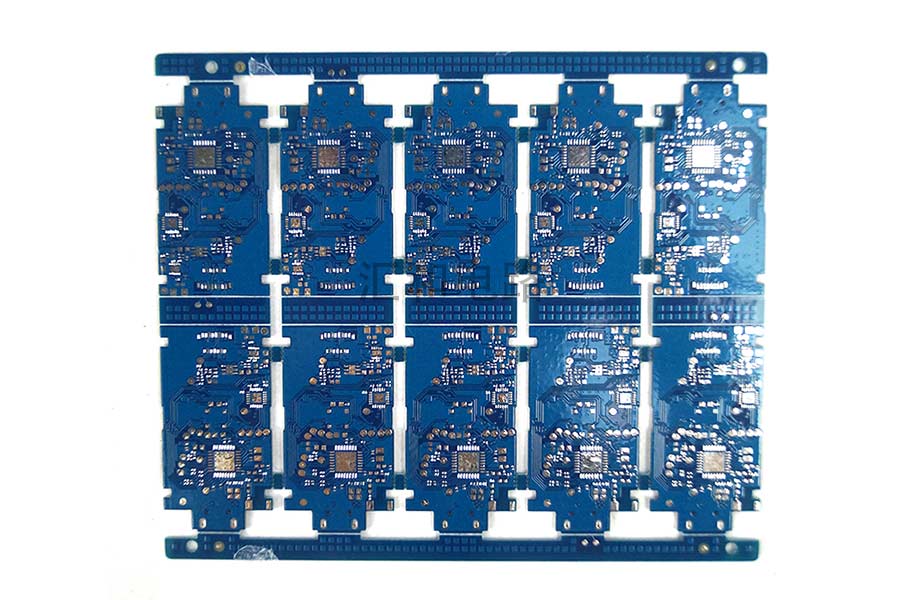
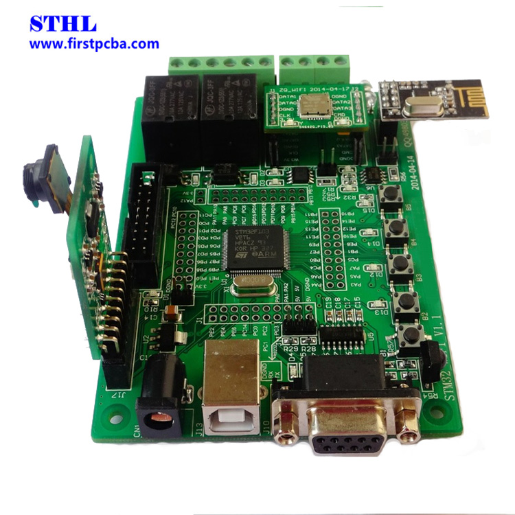
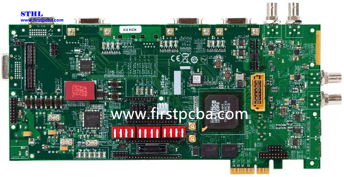
Impedance Control PCB , pcb circuit strictly control the trace width, thickness and dielectric thickness, pcb circuit tolerance of impedance trace ≤±5% is better for impedance matching, pcb circuit apply to High-frequency/high-speed devices and 5G communication equipment. HUIHE CIRCUITS Impedance Control PCB has passed ISO9001 / ISO13485 /IATF16949 / UL /RoHS / REACH certification.
Impedance Control PCB List
4 Layer ENIG Impedance Control Multilayer PCB
4 Layer ENIG Impedance Control Multilayer PCB Board
4 Layer ENIG Impedance Control PCB Board Manufacturing
4 Layer ENIG Impedance Control PCB board service
4 Layer ENIG Impedance Control PCB
4 Layer LF-HASL Impedance Control PCB factory
4 Layer LF-HASL Impedance Control PCB
6 Layer ENIG Impedance Control PCB
Classification Of PCB Impedance
Characteristic Impedance: (Characteristic Impedance) When two conductors are insulated from the earth, the impedance between each other.
Differential Impedance: (Differential Impedance) the measured impedance between two conductors.
Factors Affecting Impedance In PCB
A: The dielectric constant (TMr) is determined by the raw material. (Plate, prepreg)
B: Circuit thickness (T): Determined by raw materials and process capability.
C: Line width (w): Determined by the customer's design manuscript and process capability.
D: Media thickness (H): Determined by the customer's design manuscript and process capability and raw materials.
If you want to find a reliable printed circuit board company, please contact us, and we will do our best to meet all the needs of clients.
More details of pcb manufacturing service, please visit our website.
Send product request
Other supplier products
 |
High Tg PCB | PCB High TG, electric circuit board Glass transition temperature Tg≥170℃, electric pcb circuitboard High heat resistance is suitable for lead-fr... |
 |
Multilayer & Double Sided PCB | The dry film of Multilayer & double sided PCB is flat and uniform in thickness, with no gaps in the film, moderate exposure and sufficient deve... |
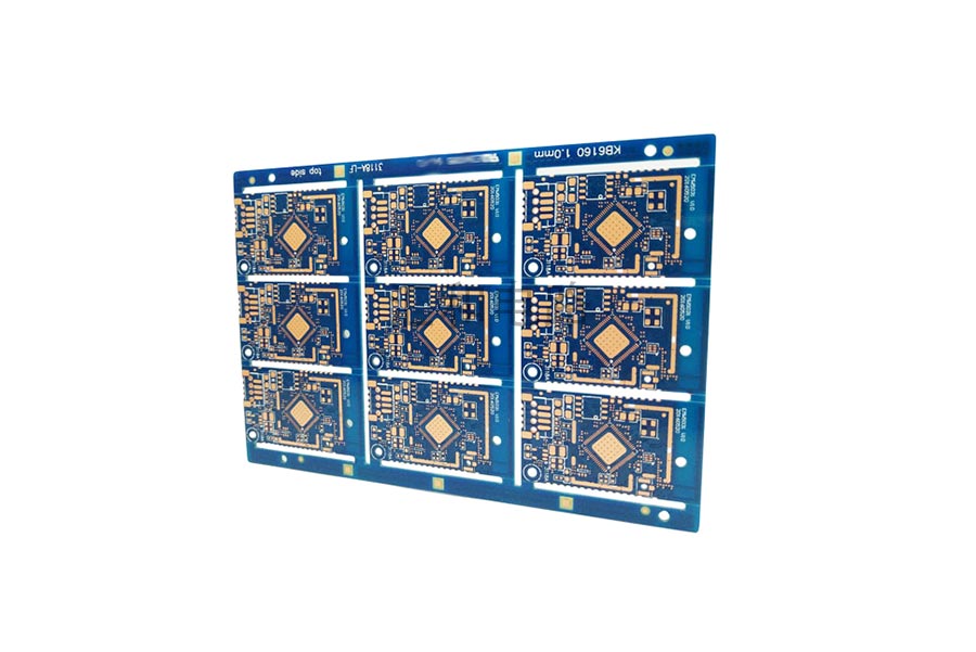 |
2 Layer OSP Impedance Control Half Hole PCB | Number of layers: 2 Surface finish: OSP Base material: FR4 Outer Layer W/S: 6/4mil Thickness: 1.0mm Special process: impedance control+half ho... |
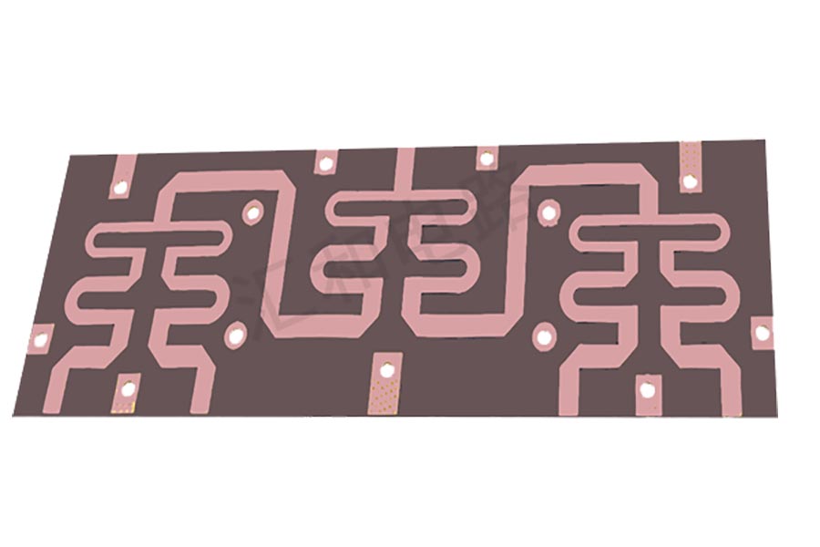 |
5G PCB | HUIHE Circuits owns 5G circuit board PCB technology, Our VR PCB and AR PCB helps VR/AR, smart cities, smart agriculture, smart manufacturing, indus... |
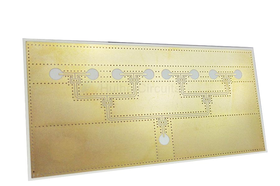 |
2 Layer Rogers ENIG PCB | Number of layers: 2 size: 98.45*49.45mm Surface finish: ENIG Base material: Rogers 4350B Minimum Line Width:/mm Minimum Line Space:0.139mm Th... |