Pcb Electronics


PCB Knowledge:PCB surface treatment technology refers to form a layer that it is different from the mechanical, physical and chemical properties of the substrate on PCB components and electrical joints. The aim is to ensure good solderability or electrical properties of PCB. Because copper tends to exist in the form of oxides in air, the solderability and electrical properties of PCB are seriously affected, so the surface treatment of PCB is needed.(pcb electronics)Process of pcb manufacturing:PCB Capability:Max layers number:40 layersMin line width/gap:3mil/3milMin hole size for mechanical drill:0.15mmMin hole size for laser drill:0.1mmMin annular ring:4 milMax copper thickness:12ozMax size for single and double layers PCBs:600 x 1200mmMax size for multi-layers PCBs:500 x 1200mmBoard thickness for 2 layers:0.2-7.0mmBoard thickness for multi-layers:0.4-7.0mmMin solder mask bridge:0.08mmAspect raion:15:1Plugging vias capability:0.2-0.8mmImpedance Control Tolerance:±10%Thickness tolerance for PTH:+/- 3milThickness tolerance for NPTH:+/- 2milSolder mask color:White,black,blue,green,yellow, red and so onCharacter:White,yellow,black.Finished surface:OSP(Entek),HASL no lead free lead free HASL,ENIG(Immersion Gold), mmersion Tin,Immersion Silver, Hard Gold,Platting Gold, Gold Finger,Enepig.Month capability:5000 types/month. 6000m2/monthNormal board materials:SHENGYI,ITEQ,KB.Special materials:ROGERS,ARLON,TACONIC,NELCO, ISOLA,HighTG:S1000-2.IT180PCB Equipment:Certifications:Our Company is UL,ISO9001,ROHS and GJB9001B certified.Packing and Shipping:FAQ:1. How to Get a quotation?For PCBs,pls send us the Gerber File.For PCBA,pls send us the Gerber file and BOM(Bill of Materials)2. What is the MOQ?No MOQ.1 pcs is ok.3.What is the lead time?For PCB orders,the lead time is 2 to 10 days.For PCBA orders,the lead time will be 15 to 30 days.4.Will the boards be tested before shippment?Yes,all PCBs will be tested by Flying Probe or E-test.For PCBA,we will have AOI,X-ray,and functional test
Другие товары поставщика
|
|
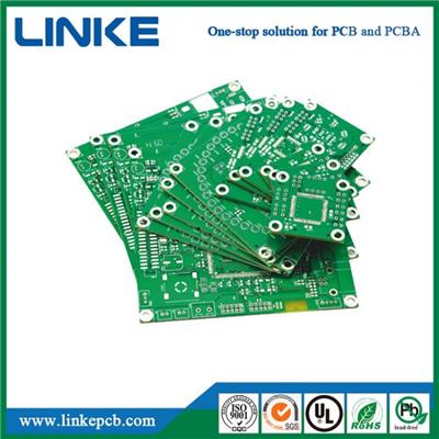
Pcb China |
Our Services:PCB Design PCB Manufacture (1-40 layers,FR4,High TG,Rigid-flex PCB,Aluminium) Components Sourcing (100% guarantee original parts from ... |
|
|
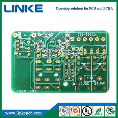
Pcb Electronics |
PCB Knowledge:PCB surface treatment technology refers to form a layer that it is different from the mechanical, physical and chemical properties of... |
|
|
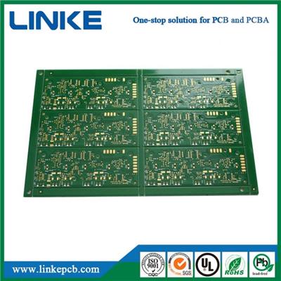
Pcb Manufacturing |
PCB Knowledge:According to the layout of the circuit module, the related circuit that realizes the same function is called a module. The components... |
|
|
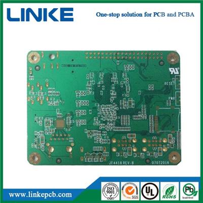
Pcb Fabrication |
PCB Knowledge:Of all surface treatments, HASL (lead free / no lead free) is the most common and cheapest treatment, but note the RoHS rules of the ... |
|
|
Pcb Board |
Our Services:
PCB Design PCB Manufacture (1-40 layers,FR4,High TG,Rigid-flex PCB,Aluminium) Components Sourcing (100% guarantee original... |
Все товары поставщика
Похожие товары