Controlled Impedance 6L/1.6mm HDI PCB in Mobile with blind and buried holes


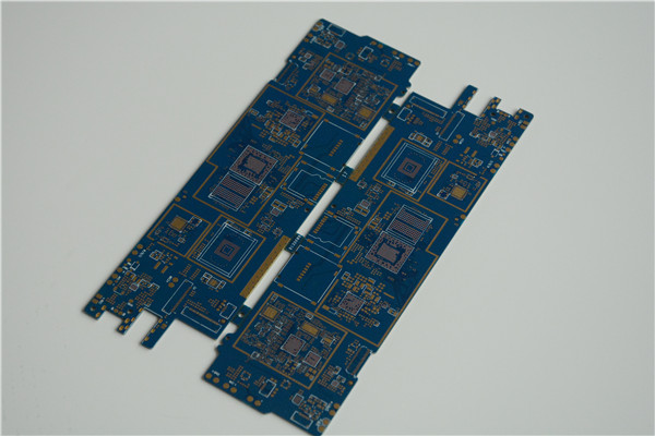
Application Field: Mobile
Layer/Board Thickness:6L/1.6mm
Surface Treatment: ENIG+OSP
Line/Space: 3.5/3.5mil
Smallest Hole Diameter:0.15mm
Technical Feature: 1+4+1, impedance control blind and buried holes
Отправить запрос, связаться с поставщиком
Другие товары поставщика
 |
Rigid 2L/1.6mm Hardware Systems Design PCB in Consumer electronics | Application Field: Consumer electronics Layer/Board Thickness: 2L/1.6mm Surface Treatment: Hard gold 30u” Technical Feature: Hard gold surfac... |
 |
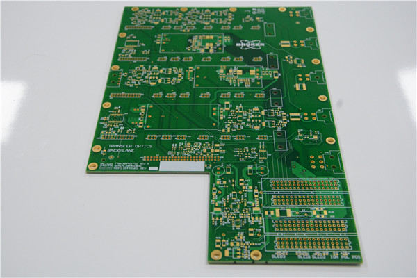
Electronics Automotive 10L/3.2mm HDI PCB Chinese manufacturer | Application Field: Consumer electronics Layer/Board Thickness: 10L/3.2mm Surface Treatment: ENIG Line/Space: 4/4mil Smallest Hole Diameter:0.15mm T... |
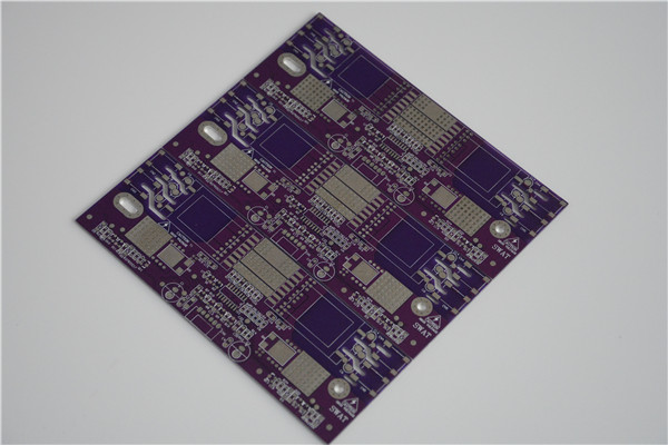 |
HDI 4L/1.6mm PCB in power with 2OZ Purple Chinese factory | Application Field: power Layer/Board Thickness:4L/1.6mm Surface Treatment: LF-HASL Line/Space: 8/8mil Smallest Hole Diameter:1.0mm Technical Featur... |
 |
Global Sourcing Multilayer Manufacturability PCB equipment manufacturers | Application Field: Consumer electronics Layer/Board Thickness: 4L/1.6mm Surface Treatment: ENIG Line/Space: 5/4mil Smallest Hole Diameter: 0.3mm Te... |
 |
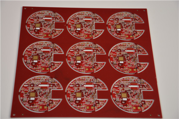
energy and gas metering equipment Rigid PCB with AutoID &RFID & RTLS technologies | Application Field: Consumer electronics Layer/Board Thickness: 4L/1.6mm Surface Treatment: ENIG3u” Line/Space: 8.0/8.0mil Smallest Hole Diame... |