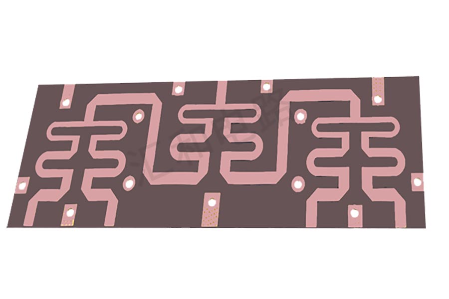
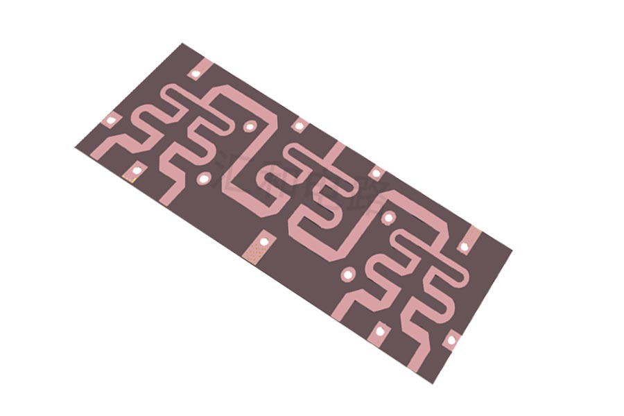
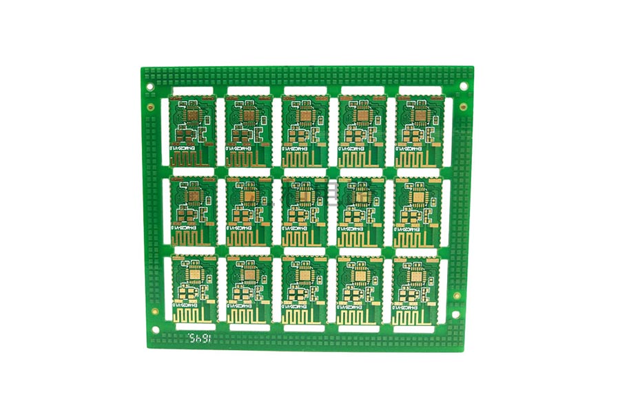
2 Layer Rogers LF-HASL PCB


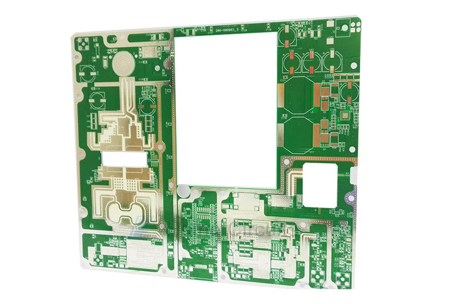
Number of layers: 2
size: 184.2*158.9mm
Surface finish: LF-HASL
Base material: Rogers 4350B
Minimum Line Width: 0.227mm
Minimum Line Space: 0.127mm
Thickness: 0.7mm
Advantages Of 2 Layer Rogers LF-HASL PCB
Own lamination process to convenient production for Multilayer PCBand shorten the lead time.
Jiangxi facility is environmental-friendly approved by the government .
Famous raw materials brand, Kingboard, Shengyi, ITEQ, Taiyo, Guangxin.
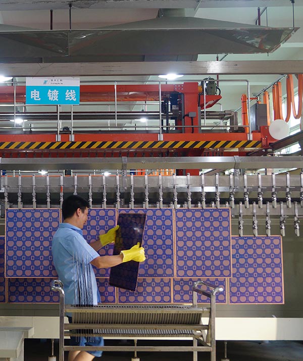
Highly automated production line with AIO Optical Scanning, Electroplating Automatic Line, High-speed flying probe test machines and inkjet printer.
Engineers with more than 15 years of experience
The management level is highly educated, 30% have professional titles and more than ten years of work experience.
High staff stability, low mobility.
UL/ISO9001/SGS/IATF16949/ROHS/ISO1400 certificated.
Sales office in Shenzhen and own 12,000sqm factory in Jiangxi.
Establish an e-commerce system to reduce transaction costs and increase market response speed.
As one of rogers pcb manufacturers, we can offer high quality rogers pcbfor sale, andthe rogers pcb price is low, if you have needs, please contact us.
If you are looking for a reliable circuit board maker, please choose us, and we will be your best partner.
Отправить запрос, связаться с поставщиком
Другие товары поставщика
 |
High Frequency PCB | High frequency printed circuit board, High frequency pcblow dielectric constant, high transmission rate, high frequency pcb low dissipation factor,... |
 |
2 Layer F4B ENIG PCB | Number of layers: 2 Surface finish: ENIG Base material: F4B Outer Layer W: 6mil Outer layer S: 6mil Thickness: 1.0mm Advantages Of 2 Layer F4... |
 |
Consumer PCB | The size, thickness and weight of products in the consumer electronics field have been greatly reduced. Via in pad PCB, blind buried vias PCB, half... |
 |
PCB Board | As aprofessionalpcb manufacturing company, HUIHE Circuits has mastered advanced technology in the PCBindustry, we own reliable production equipment... |
 |
PCB Prototyping | 97% On-Time Delivery Ratio In accordance with IPC standards, high quality pcb prototype manufacturer strictly control the qualified rate of finishe... |