

Half Hole & Through Hole Pcb

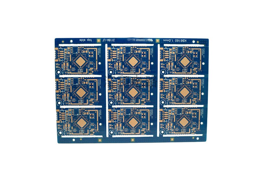
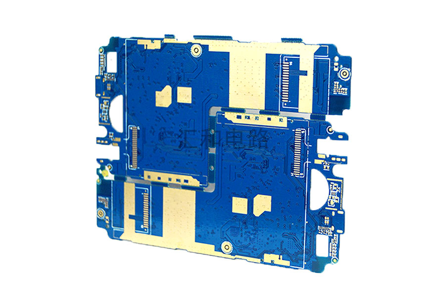
Through hole circuit board& half hole PCB, no copper burr residue or warpage in half hole, reduce connectors and save space, apply to Bluetooth module and Signal receiver products. HUIHE CIRCUITS PCB board with holesapply to Bluetooth module and Signal receiver products. Our PCBproducts have passed ISO9001/ISO13485/IATF16949/UL/RoHS/REACH certification.
Half Hole & Through Hole PCB List
2 layer OSP impedance control half hole PCB
2 layer ENIG half hole PCB
4 layer ENIG impedance control half hole PCB electric circuit board
2 layer ENIG impedance control half hole PCB
8 layer ENIG half hole custom PCB
4 layer ENIG impedance control half hole fr4 PCB
4 layer ENIG impedance control half hole PCB
4 layer LF-HASL half hole PCB
Production Process Of Metallized Half-Hole PCB
For the front inversion, to prevent the quality of the product and the need to make corrections in the later process, the production process of this type of board is processed according to the following process: a drilling (drilling, gong groove-plate surface plating-external Optical imaging-pattern plating-co-drying-half-hole processing-film stripping, etching, tin stripping-other processes-shape
Main Points Of Metallized Half-Hole PCB Production
The specific metallized PCB half holes are processed in the following way: all metallized half-hole PCB holes must be drilled in the pattern after plating, and one hole at the intersection of the two ends of the half-hole should be drilled before etching.
The engineering department formulates the MI process according to the process
The metal half-hole is the second-drilled half-hole drilled during the first drilling (or gong), after the image is plated, and before the etching. It is necessary to consider whether the copper will be exposed when the gong groove is shaped, and move the drilled half-hole into the unit.
he right hole is drilled first, and then the board is turned over (or mirrored) and the left hole is drilled to reduce the pulling of the copper of the inner hole of the half hole by the drill, resulting in the lack of copper of the hole.
The size of the drill nozzle for drilling the half hole depends on the spacing of the contour lines.
Draw the solder mask film, use the gong space as a stop point and open the window to increase 4mil treatment.
The Designer's Suggestion When Designing The Circuit
Change the distance from the edge line to the hole center. The general design is to place the hole center on the edge line and move the control center down. For example, the diameter of the hole is 1.4mm, the distance between the two holes is 2.54mm, and the board edge The distance between the line is 0.33mm from the center of the through hole, and the thickness of the plate is 0.6mm. The angle between the tangent to the cut point of the wall and the track of the milling cutter was 90 degrees before, but this time it is about 60 degrees. Because the board edge line is at a certain distance from the center of the through hole, the cutting angle of the milling cutter is changed, and the board thickness is extremely small, so the copper in the hole is not easily pulled out. The simultaneous improvement of small batch pcb design and production can greatly improve the production yield of PCB half-hole boards.
As a pcb board maker, we will do our best to meet all the needs of customers.
Send product request
Other supplier products
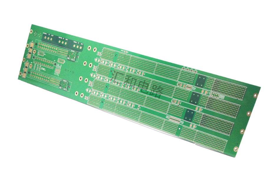 |
High Tg PCB | High TG PCB, electric circuit board Glass transition temperature Tg≥170℃, electric circuit board High heat resistance is suitable for lead-free ... |
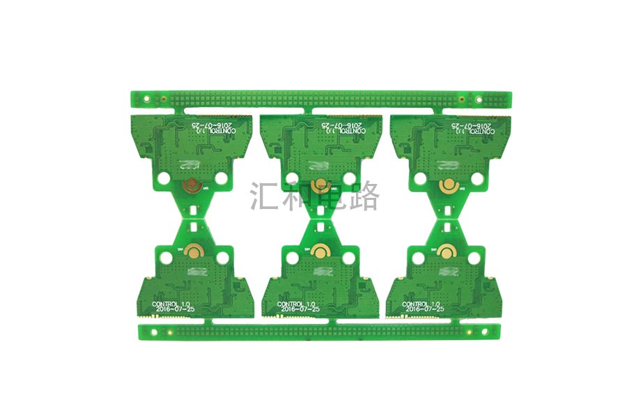 |
2 Layer ENIG Impedance Control Half Hole PCB | Advantages of 2 layer pcb board Own lamination process to convenient production for Multilayer PCB and shorten the lead time. Jiangxi facility is... |
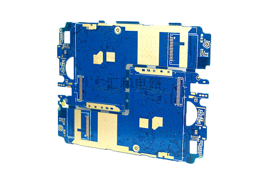 |
2 Layer Taconic ENIG PCB | Number of layers: 2 Surface finish: ENIG Base material: Taconic TLY-5A Outer Layer W: 1.046mil Outer layer S: /mil Thickness: 0.94mm Advant... |
 |
PCB Application | As a leading PCB supplierin China printed circuit board industry, HUIHE Circuits PCB board applicationincluding communications, computers, industri... |
 |
4 Layer High TG Impedance Control Fine Pitch PCB | Number of layers: 4 Surface finish: ENIG Base material: High TG FR4 Outer Layer W/S: 4/3.5mil Inner layer W/S: 4/3.5mil Thickness: 1.0mm Spec... |
Same products
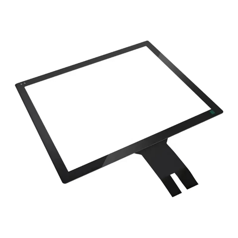 |
15 Inch Capacitive Touch Screen Panel for Medical & Multi-Application Equipment | Seller: SEMIJEI TECHNOLOGY LTD | 15 Inch Capacitive Touch Screen Panel for Medical & Multi-Application Equipment 15 Inch Ca... |
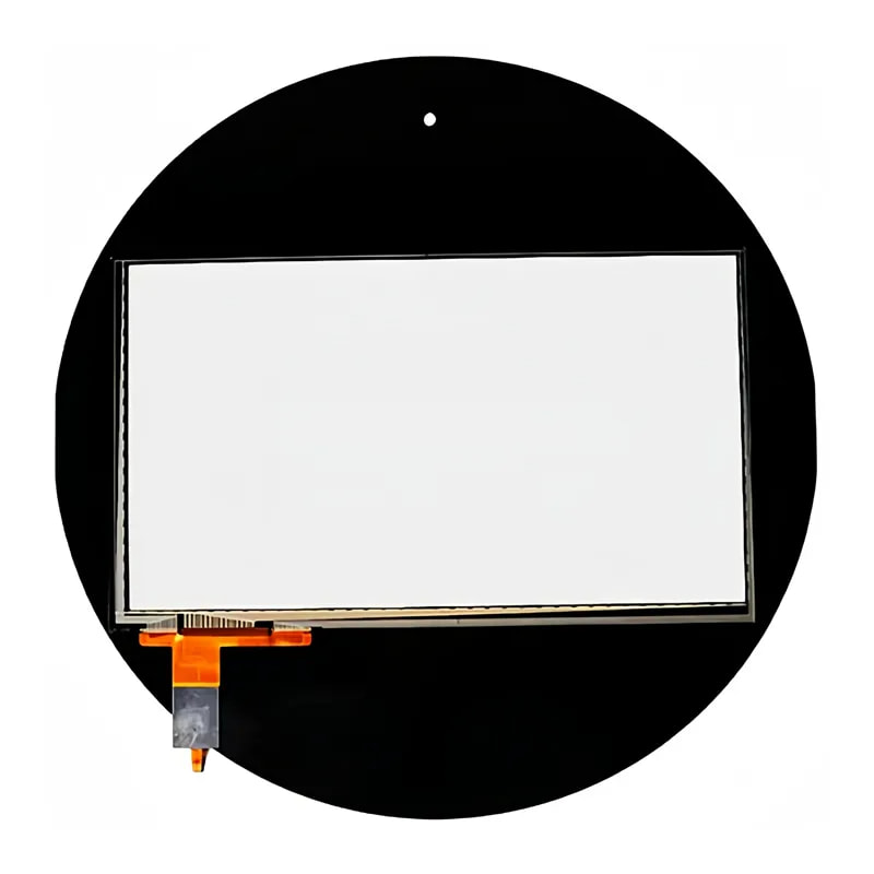 |
Custom Size 11.6 Inch Circular Shape Touch Screen With ILITEK Controller | Seller: SEMIJEI TECHNOLOGY LTD | Custom Size 11.6 Inch Circular Shape Touch Screen With ILITEK Controller Semijei-Tech's11.6 in... |
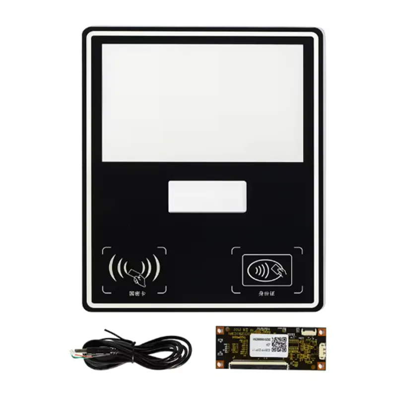 |
10.6 Inch Custom Shape Touch Screen With Multi-Touch for Commercial Systems | Seller: SEMIJEI TECHNOLOGY LTD | Semijei-Tech's10.6 inch custom shape touch screenis a projected capacitive touch panel develope... |
 |
Semijei-Tech's 10.1 inch | Seller: SEMIJEI TECHNOLOGY LTD | Semijei-Tech's10.1 inch waterproof mirror glass multi-touch panelcombines projected capacitive ... |
 |
7" I²C Glove Touch Capacitive Touch Panel | Seller: SEMIJEI TECHNOLOGY LTD | 7" I²C Glove Touch Capacitive Touch Panel 7 Inch Glove Touch Capacitive Touch Panelfor In... |

