GAN ON SAPPHIRE
Brief Introduction of GaN
GaN is the major material used for blue-light/green-light LED due to its ability to combine electrical parts and LED optical parts, increasing LED product efficiency.
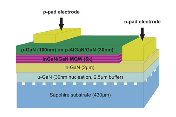
The GaN-based LEDs grown on the sapphire substrate have current transport along the lateral direction due to the insulating nature of the substrate. In addition, the finite resistance of the n-type GaN buffer layer causes the p–n junction current to be nonuniform and crowds near the edge of the contact.
The most frequently chosen crystallographic planes have been the R-plane, C-plane, and A-plane of sapphire. The tremendous mismatch between the lattices of GaN and sapphires can be partly overcome by the use of thin buffer layers of AlN or GaN. In spite of the lattice-matching problem, many useful optoelectronic and electronic devices can be made.
Characteristics and Applications of GaN
GaN is the third-generation semiconductor material after silicon and gallium arsenide. Its wide-bandgap characteristics make that GaN is an ideal material for blue light output. In addition, GaN also has a small dielectric constant, excellent thermal conductivity and thermal stability, which can meet the requirements of high frequency, high temperature, high pressure and high power applications.
These properties make GaN in aerospace, satellite communications, storage display, new type Light source and nuclear energy development have a wide range of application prospects. However, the bottleneck that once limited the application of GaN was the growth process of GaN, and the key to the growth process was the choice of substrate materials.
Cryscore GaN on Sapphire
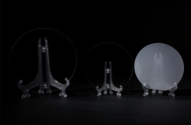
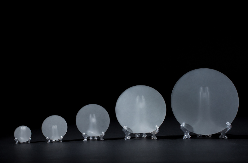
Although there is a large lattice fit between the sapphire crystal and the GaN crystal, the crystal structures of the two are the same, and the sapphire still maintains stable chemical properties at high temperatures. In addition, for its excellent heat dissipation performance, sapphire wafer can be used as GaN Ideal substrate material for growth processes. Growing GaN on a sapphire substrate is easy to obtain large-size epitaxial wafers, and the price is relatively cheap.
With the development and improvement of molecular beam epitaxy and chemical vapor deposition growth technology, the quality of epitaxially growing GaN crystals on sapphire is getting higher and higher.
If you are interested in our products, contact us now to get more info about the price of sapphire waferand sapphire substrate.
CRYSCORE OPTOELECTRONIC LIMITED has been a professional manufacturer specialized in high-quality sapphire wafers and sapphire opticswindows since 2008.
在线联系供应商
Other supplier products
| PATTERNED SAPPHIRE SUBSTRATES | Sapphire wafer is the most widely used substrate material in semiconductor lighting industry, and pattern sapphire substrate(PSS) is the general me... | |
| R-PLANE (1-102) SAPPHIRE WAFERS | R plane(1-102) sapphire wafers are preferred for the hetero-epitaxial deposition of silicon used in microelectronic IC applications. R plane is the... | |
| CUSTOM SAPPHIRE WAFERS | CRYSCORE supplies sapphire wafers with the high-quality surfaces in all orientations (C-plane, A-plane, R-plane, sapphire m plane, N-plane, V-plane... | |
| SAPPHIRE INGOTS/RODS | SAPPHIRE INGOTS/RODS Sapphire ingots are typically used as raw materials for further processing. These sapphire rod and sapphire ingots are uniform... | |
| Silicon on Sapphire | As a professional sapphire wafermanufacturer, CRYSCORE can provide standard or optical sapphirewafers with any orientation applied to epitaxy, as w... |
Same products
| Fischer Tropsch wax white granules used in candle | 卖方: Syntop chemical Co.,Ltd. | Fischer-Tropsch wax is used in various formulations of hot-melt adhesives: Low-temperature/high-... | |
| Mining Machinery Parts | 卖方: XINGTAI ME MINING EQUIPMENT CO.,LTD. | Mining Machinery Parts HEAVY-DUTY MINING EQUIPMENT PARTS SUPPLIER Mining Equipment Parts ... | |
| PH-08 Waterproof Soil PH Meter | 卖方: 科立龙电子股份有限公司 | Model PH-08 Range PH 0.00~14.00PH Temp 0~50℃ Resolution PH 0.01PH Temp 0.1℃ Accuracy PH ±... | |
| candle raw material White Wax with low melting point | 卖方: Syntop chemical Co.,Ltd. | Lubricant wax: Fischer-Tropsch wax is widely used in the lubricants sector. It offers excellent l... | |
| Fischer Tropsch wax used for road marking paint | 卖方: Syntop chemical Co.,Ltd. | Fischer-Tropsch wax is widely used in road marking paints and serves as a key performance additiv... |


