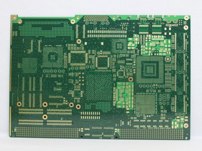
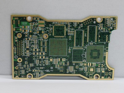
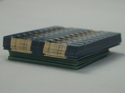
Blind & Buried VIA Hole PCB


Custom blind and buried vias fabricationfrom professional and experienced PCB board supplier at low cost.
First, we start with traditional multi-layer boards. The structure of a standard multi-layer circuit board is a process including an inner layer line and an outer layer line, followed by drilling, and metallization in the hole to achieve the internal connection function of each layer line. However, due to the increase in line density, the way parts are packaged is constantly updated. In order to allow for a wider board area, more high-performance parts can be placed. In addition to the thinner line width, the aperture is also reduced from 1 mm in the DIP jack to 0.6 mm in SMD, and further reduced to 0.4 mm or less. However, the surface area is still occupied, so that there are buried holes and blind holes.
HDI PCB
HDI PCB
HDI boards, one of the fastest growing technologies in PCBs, are now available at PCBSky. HDI Boards contain blind and/or buried vias and often contain microvias of .006 or less in diameter. They have...
The Buried Holes and Blind Holes are Defined as Follows
Blind Vias: A blind via is a type of via that connects the inner trace of the PCB to the trace of the PCB surface. This hole does not penetrate the entire board.
Buried Vias: Buried vias are only connected to the type of vias between the inner layers, so they are not visible from the surface of the PCB.
Advantages of Blind Buried Hole Printed Circuit Board
Eliminate a large number of through-hole designs and increase wiring density and package density;
Diversify and complicate the design of the interconnect structure of the multi-layer board;
Significantly improved the reliability of multi-layer boards and the electrical performance of electronic products.
The Following Three Points are Distinguished for Blind Buried Plate Boards
In contrast to the through hole, the through hole refers to a hole through which each layer is drilled, and the blind hole is a non-drilled through hole.
Blind and buried viasubdivision: blind hole, buried hole (outer layer is not visible).
Distinguish from the production process: blind holes are drilled before pressing, and through holes are drilled after pressing.
Blind buried hole technology is mainly used on relatively high-end PCBs, with high technical content and high requirements for blind hole PCBboard manufacturers.
CHINA CUSTOM PCBFABRICATION
PCBSKY is a professional PCB/FPC manufacturer in China, providing full PCB fabrication services in certified quality standards. We specialize in quick turn PCB & prototypes.
Send product request
Other supplier products
 |
HDI PCB | HDI PCBs, one of the fastest growing technologies in PCBs, are now available at PCBSky. HDI PCBs contain blind and/or buried vias and often contain... |
 |
High Tg PCB | What is High Tg PCB When the temperature rises to a certain area, the substrate will change from "glass state" to "rubber state", and the temperatu... |
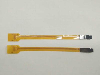 |
Double Sided Flexible PCB | After the double-sided PI board copper-clad board material is used in the double-sided circuit, a protective film is added on both sides to form a ... |
 |
High Tg PCB | What is High Tg PCB When the temperature rises to a certain area, the substrate will change from "glass state" to "rubber state", and the temperatu... |
 |
Edge Plating/Half-hole PCB | Half hole pcb: The walls of the PTH holes on the PCB are plated with Half-hole formed by smooth and complete metal forming.The Half hole process on... |