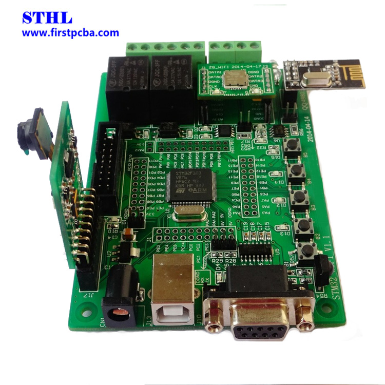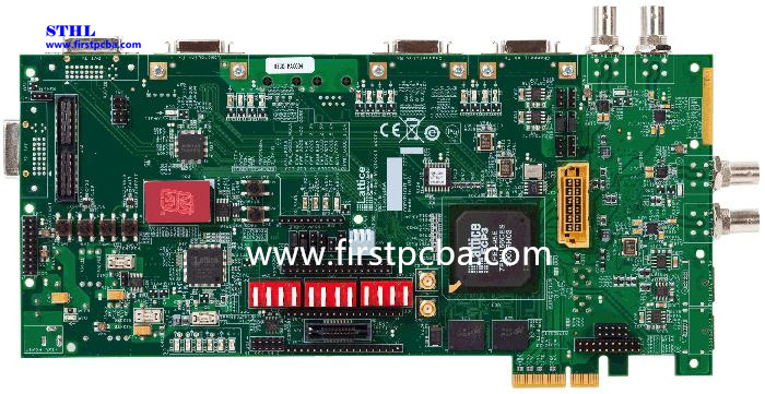
2 Layer Rogers ENIG PCB

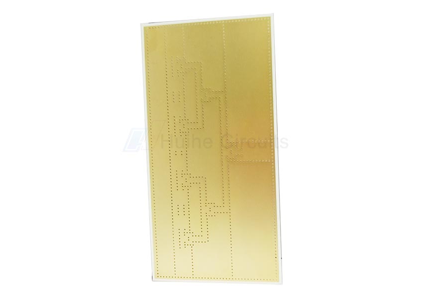
Number of layers: 2
size: 98.45*49.45mm
Surface finish: ENIG
Base material: Rogers 4350B
Min. hole diameter: 0.5mm
Minimum Line Width:/mm
Minimum Line Space:0.139mm
Thickness: 0.35mm
Advantages Of 2 Layer Rogers PCB
Own lamination process to convenient production for Multilayer PCB and shorten the lead time.
Jiangxi facility is environmental-friendly approved by the government .
Famous raw materials brand, Kingboard, Shengyi, ITEQ, Taiyo, Guangxin.
Highly automated production line with AIO Optical Scanning, Electroplating Automatic Line, High-speed flying probe test machines and inkjet printer.
Engineers with more than 15 years of experience
Customers located in more than 20 countries, the common choice of 500 high-end companies.
High staff stability, low mobility.
UL/ISO9001/SGS/IATF16949/ROHS/ISO1400 certificated.
Sales office in Shenzhen and own 12,000sqm factory in Jiangxi.
Establish an e-commerce system to reduce transaction costs and increase market response speed.
If you have needs to buy rogers ro4350b pcb, please contact us.
As a custom pcb manufacturer, we can offer kinds of pcb boards for sale, anything you need, please contact us.
Send product request
Other supplier products
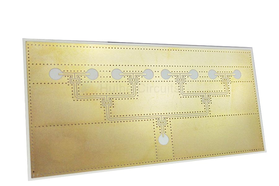 |
2 Layer Rogers ENIG PCB | Number of layers: 2 size: 98.45*49.45mm Surface finish: ENIG Base material: Rogers 4350B Minimum Line Width:/mm Minimum Line Space:0.139mm Th... |
 |
Consumer PCB | Consumer PCB The size, thickness and weight of products in the consumer electronics field have been greatly reduced.In-disk hole plate, blind burie... |
 |
Industrial Control PCB | With the continuous development of the “pcb automationequipment + industrial robot operation” mode,The requirements for electronic and ... |
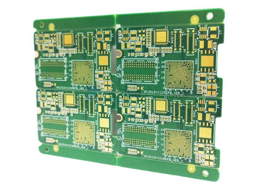 |
10 Layer ENIG Blind Vias PCB | Number of layers: 10 Surface finish: ENIG Base material: FR4 W/S: 4/4mil Thickness: 1.6mm Special process: Blind Vias Advantages Of 10 Layer ENIG ... |
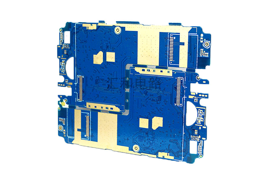 |
4 Layer High TG Impedance Control Fine Pitch PCB | Number of layers: 4 Surface finish: ENIG Base material: High TG FR4 Outer Layer W/S: 4/3.5mil Inner layer W/S: 4/3.5mil Thickness: 1.0mm Spec... |