

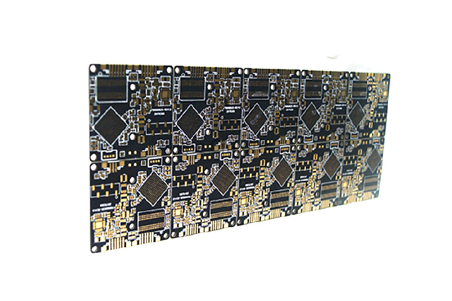
Via In Pad Fr4 PCB


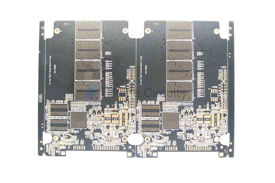
Via In pcb board material fr4, using copper plating or epoxy to fill holesfor circuit board factor, prevent solder paste or flux from flowing into the via in pad, avoid solder ball getting into via or solder mask cover on pad and cause false soldering. HUIHE CIRCUITS Via In Pad Fr4 PCB has passed ISO9001/ISO13485/IATF16949/UL/RoHS/REACH certification.
What Is A Hole-In-The-Panel Circuit Board?
The hole in the disk is an important part of the multi-layer PCB. It is not only responsible for the main functions of the PCB, but also the cost of drilling usually accounts for 30% to 40% of the PCB manufacturing cost. In short, the holes pressed on the pads on the PCB can all be called holes in the disk.
Processing Requirements For Hole Plugs In The Disk
No solder mask ink entering the hole
There should be no tin beads hidden in the hole
No explosive oil, ink pads, making it difficult to mount components, etc.
Common Sense Of Circuit Board Plug Hole
Prevent the tin from penetrating the component surface from the via hole to cause a short circuit when the PCB is wave soldered
Avoid flux residue in the vias
Prevent the tin balls from popping up during wave soldering, causing short circuits
Prevent surface solder paste from flowing into the hole, causing false soldering and affecting placement
Huihe Circuits is a professional pcb circuit manufacturer, we provide fr4 circuit board material, fr4 circuit board manufacturing, fr4 pcb board, fr4 pcb datasheet, fr4 pcb sheet, fr4 pcb thickness, pcb manufacturing serviceand etc. For more information, please feel free to contact us!
Отправить запрос, связаться с поставщиком
Другие товары поставщика
 |
4 Layer FR4+Rogers ENIG PCB | Number of layers: 4 size:80*88mm Surface finish: ENIG Base material: Rogers FR4 4350B Min. hole diameter: 0.3mm Minimum Line Width:0.230mm Minimum ... |
 |
4 Layer FR4+Rogers ENIG PCB | Number of layers: rogers fr4 size:80*88mm Surface finish: ENIG Base material: FR4+Rogers 4350B Minimum Line Width:0.230mm Minimum Line Space:0... |
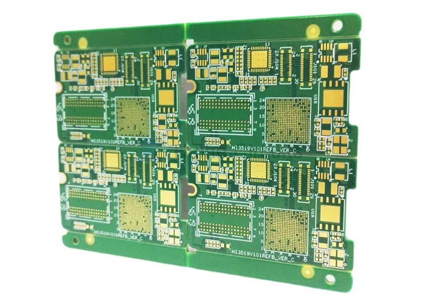 |
10 Layer ENIG Blind Vias PCB | Number of layers: 10 Surface finish: ENIG Base material: FR4 W/S: 4/4mil Thickness: 1.6mm Special process: Blind Vias Advantages Of 10 Layer ENIG ... |
 |
8 Layer ENIG Impedance Control PCB | Number of layers: 8 Surface finish: ENIG Base material: FR4 Outer Layer W/S: 4/3mil Inner layer W/S: 4/3mil Thickness: 1.2mm Special process:... |
 |
Rail Transit PCB | Huihe Circuits has extensive experience in manufacturing customized subway pcbfor customers in the railway, rail transit and automotive industries.... |
Похожие товары
 |
Air insulated Dry type transformer VPI | Продавец: Power transformer | Air insulated Dry type transformer VPI TAILI SG(B) air-barrier dry-type transformer( VPI) is des... |
 |
Cast Resin Dry Type Transformer with Cooling Fan | Продавец: Power transformer | Cast Resin Dry Type Transformer with Cooling Fan Taili’s advanced epoxy resin casting pr... |
 |
1250kVA Dry type Transformer for Bangladesh | Продавец: Power transformer | 1250kVA Dry type Transformer for Bangladesh Taili's advanced epoxy resin casting process ensures... |
 |
35kV Dry-type transformer with OLTC | Продавец: Power transformer | 35kV Dry-type transformer with OLTC Taili's35kV Dry-type Transformer with OLTC (On-Load Tap Chan... |
 |
Cast Resin Dry Type Transformer | Продавец: Power transformer | Cast Resin Dry Type Transformer IEC/ANSICast Resin TransformersfromTAILI Electric, is difference... |
