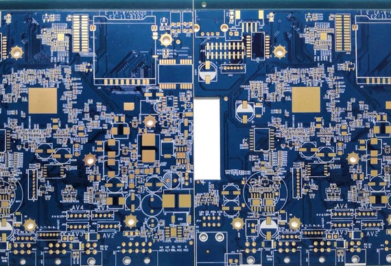
WIRING ON THE DOUBLE-SIDED BOARD——DOUBLE SIDED PCB


Speedapcb - The printed circuit board manufacturersin China, established in 2014, is located in Changsha, Hunan Province. The company focuses on high-speed PCB design, printed circuit board manufacturing, SMT welding processing, and supply chain services. Products are widely used in communications equipment, computers and network equipment, consumer electronics, automotive electronics, industrial control, new energy, rail transportation, and other industries.
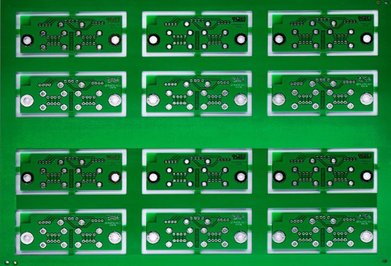
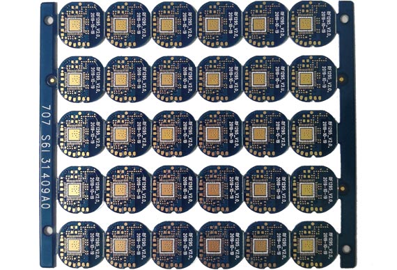
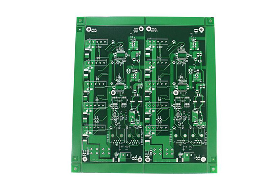
There are wiring on both sides of the dual layer PCB, but to use the wires on both sides, you must have a proper circuit connection between the two sides. This "bridge" between circuits is called a via. A via is a small hole filled or coated with metal on the two sided pcb. It can be connected to the wires on both sides. Because the area of the double-sided board is twice as large as the single-sided board, the dual layer PCB solves the difficulty of wiring interleaving in the single-sided board (which can be conducted to the other side through the hole), and it is more suitable for more complicated circuits than the single-sided board.
HAVE A QUESTION OR REQUEST?
Click below, we’ll be happy to assist.
SPEEDAPCB is a professional PCB supplier. We can provide customers with a one-stop service from PCB design to PCB production and assembly.
As a professional PCB manufacturer, we have 10 PCB production lines to manufacture double sided prototype pcb. The machine works 24 hours a day, only to provide customers with satisfactory delivery time.
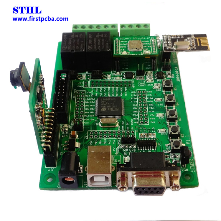
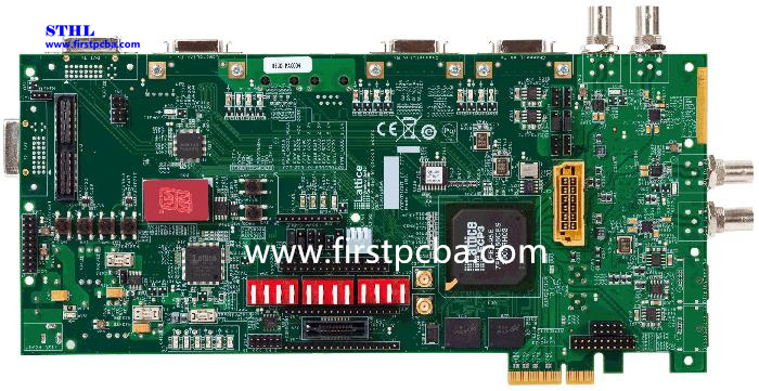
Our PCB boards can be divided into single-panel double-panel and multilayer boards according to their structure. Thedouble sided circuit boardis a board with double-sided wiring on the board. An important feature of the double sided prototype PCB is that it has a guide hole to connect the wires on both sides into a circuit.And now the double sided pcb priceis reasonable.
The double-panel wiring can be staggered with each other, which is the biggest difference from a single-panel; the double-panel is more suitable for complex circuits and has a wider range of use.
The cost of single and double panels is not much different. If there is no special requirement, all industries will give preference to double panels; after all, the performance and stability of double panels are better than single panels.
Parameters of Double Sided PCB
|
Item |
Capabilities |
|
|
Number of Layers |
Double Side |
|
|
Material |
FR-4,CEM-3,HighTg, Aluminum, |
|
|
Halogen Free |
||
|
PCB Thickness |
||
|
Surface finished |
Gold Plating |
|
|
Immersion Gold(Silver) |
||
|
HAL Lead Free |
||
|
Hot Air Solder Leveling(HASL) |
||
|
Entek Coating (OSP) |
||
|
Solder Mask |
Any color Green, White,Black, Yellow, Red, Blue |
|
|
Other printing |
Gold Finger |
|
|
Carbon Print, Peelable Mask |
||
|
Solder Mask Plugged Hole |
||
|
Copper thickness |
1/ 2 oz (18 um) - 4 oz (140 um) |
|
|
Hole Size Tolerance (PTH) |
+/ -0.076mm (3 mil) |
|
|
Hole Size Tolerance (NPTH) |
+/-0.05mm (2 mil) |
|
|
Profile and V-Cut |
CNC-Routing, Stamping and Beveling, V-CUT,CNC |
|
|
Special Process |
Micro-section, Chamfer for Gold Finger |
|
|
Testing |
Electrical Testing, Controlled Impedance Testing, Flying Probe Test, X-Ray Inspection AOI Test |
|
|
Environment |
Clean room environmen , Dust-free workshop |
|
|
Transportation |
Fedex, DHL, UPS, etc. |
|
|
Files |
Gerber ,Protel ,Autocad ,Powerpcb, Orcad, etc. |
|
Description of Dual Layer PCB
Dual layer PCB, also called double sided board, it has wiring on both sides, but in order to use the wires on both sides. There must be a proper circuit connection between the two sides. This circuit between the "bridge" is called a guide hole (via). Guide holes are in the PCB, filled or coated with metal holes, which can be connected to the two sides of the wire. Because the double-sided panel is twice as large as the single-sided panel, the double-sided panel solves the difficulty of interlacing the wiring in the single-sided panel (you can pass through the hole to the other side), it is more suitable for use in more complex circuits than the single-sided panel.
Principle of Double Sided PCB Design
To get the best performance of electronic circuits, the layout of components and the layout of the wire is very important. In order to design a good quality and low cost PCB, the following general principles are suitable for single sided PCB design and double sided PCB design.
First, consider the size of the PCB size. PCB size is too large, the printed lines are long, the impedance increases, noise resistance decreases, and the cost increases; too small, it is not good heat dissipation, and the neighboring lines are vulnerable to interference. After determining the size of the PCB, then determine the location of special components. Finally, according to the functional unit of the circuit, the layout of all components of the circuit.
The wiring principles are as follows.
Solder pads
The center hole of the pad should be slightly larger than the device lead diameter. The pad is too large to form a false solder. Solder pad outer diameter D is generally not less than d + 1.2 mm, where d is the lead aperture diameter. For high-density digital circuits, the minimum diameter of the pad can be d + 1.0 mm.
Function of Double Sided Printed Circuit Board
Double sided printed circuit board has the following functions in electronic equipment:
(1) To provide mechanical support for fixing and assembling various electronic components such as integrated circuits, to realize the wiring and electrical connection or electrical insulation between various electronic components such as integrated circuits, and to provide the required electrical characteristics.
(2) To provide solder resist graphics for automatic soldering and to provide identification characters and graphics for component insertion, inspection, and maintenance.
(3) electronic equipment using printed circuit boards, due to the consistency of similar printed circuit boards, to avoid errors in manual wiring, and can achieve automatic insertion or placement of electronic components, automatic soldering, automatic detection, to ensure the quality of electronic products, improve labor productivity, reduce costs, and facilitate maintenance.
(4) Provide the required electrical characteristics, characteristic impedance and electromagnetic compatibility characteristics for circuits in high-speed or high-frequency circuits.
(5) Printed boards with internally embedded passive components provide certain electrical functions, simplify electronic installation procedures, and improve product reliability.
(6)In large-scale and ultra-large-scale electronic packaging components, it provides an effective chip carrier for miniaturized chip packaging of electronic components.
Отправить запрос, связаться с поставщиком
Другие товары поставщика
 |
PLATED THROUGH HOLE PCB / PTH PCB | PCB Via Hole/ PTH PCB There are three common types of drilled holes in the printed circuit board:pcb via plating, blind via hole, and buried via ... |
 |
LEAD FREE HASL PCB / IMMERSION TIN PCB | LEAD FREE HASL PCB / immersion tin pcb Lead-free HASL is to coat a layer of tin-lead alloy on the copper surface to prevent the oxidation of the co... |
 |
SPEEDA PCB BOARD PRODUCT | Speedapcb - The pcb supplierin China, established in 2014, is located in Changsha, Hunan Province. The company focuses on high-speed PCB design, pr... |
 |
ALUMINUM PCB / METAL CORE PCB | Speedapcb - The PCB design companyin China, established in 2014, is located in Changsha, Hunan Province. The company focuses on high-speed PCB desi... |
 |
THE MOST BASIC CIRCUIT BOARD——SINGLE SIDED PCB | Speedapcb - The best PCB manufacturersin China, established in 2014, is located in Changsha, Hunan Province. The company focuses on high-speed PCB ... |