
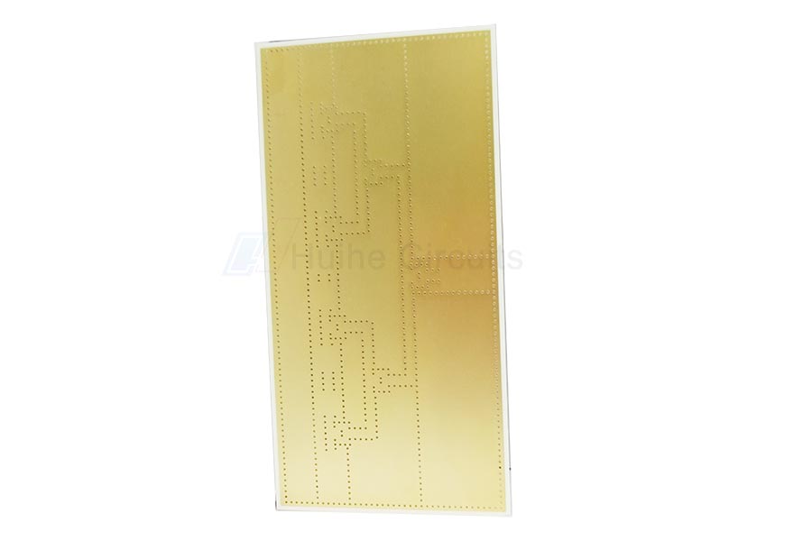
Half Hole & Through Hole Pcb

Half Hole & through hole circuit board, no copper burr residue or warpage in half hole, reduce connectors and save space, apply to Bluetooth module and Signal receiver products. HUIHE CIRCUITS Half Hole & Through Hole PCB, apply to Bluetooth module and Signal receiver products. Has passed ISO9001 / ISO13485 /IATF16949 / UL /RoHS / REACH certification.
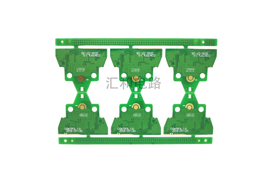
Half Hole & Through Hole PCB List
2 Layer OSP Impedance Control Half Hole PCB
2 Layer ENIG Half Hole PCB
4 Layer ENIG Impedance Control Half Hole PCB Electric Circuit Board
2 layer ENIG impedance control half hole pcb
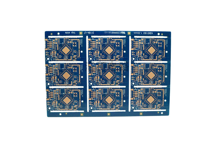
8 layer ENIG half hole custom PCB
4 layer ENIG impedance control half hole fr4 PCB
4 layer ENIG impedance control half hole PCB
4 layer LF-HASL half hole PCB
Production Process Of Metallized Half-Hole PCB
For the front inversion, to prevent the quality of the product and the need to make corrections in the later process, the production process of this type of board is processed according to the following process: a drilling (drilling, gong groove-plate surface plating-external Optical imaging-pattern plating-co-drying-half-hole processing-film stripping, etching, tin stripping-other processes-shape
Main Points Of Metallized Half-Hole PCB Production
The specific metallized half-holes are processed in the following way: all metallized half-hole PCB holes must be drilled in the pattern after plating, and one hole at the intersection of the two ends of the half-hole should be drilled before etching.
The engineering department formulates the MI process according to the process
The metal half-hole is the second-drilled half-hole drilled during the first drilling (or gong), after the image is plated, and before the etching. It is necessary to consider whether the copper will be exposed when the gong groove is shaped, and move the drilled half-hole into the unit.
he right hole is drilled first, and then the board is turned over (or mirrored) and the left hole is drilled to reduce the pulling of the copper of the inner hole of the half hole by the drill, resulting in the lack of copper of the hole.
The size of the drill nozzle for drilling the half hole depends on the spacing of the contour lines.
Draw the solder mask film, use the gong space as a stop point and open the window to increase 4mil treatment.
The Designer's Suggestion When Designing The Circuit
Change the distance from the edge line to the hole center. The general design is to place the hole center on the edge line and move the control center down. For example, the diameter of the hole is 1.4mm, the distance between the two holes is 2.54mm, and the board edge The distance between the line is 0.33mm from the center of the through hole, and the thickness of the plate is 0.6mm. The angle between the tangent to the cut point of the wall and the track of the milling cutter was 90 degrees before, but this time it is about 60 degrees. Because the board edge line is at a certain distance from the center of the through hole, the cutting angle of the milling cutter is changed, and the board thickness is extremely small, so the copper in the hole is not easily pulled out. The simultaneous improvement of small batch pcb design and production can greatly improve the production yield of pcb board with holes.
In our circuit board factory, we have types of pcb boardfor sale, if you have needs, please contact us.
在线联系供应商
Other supplier products
 |
New Energy PCB | Huihe Circuits is your ideal partner, providing you with electromechanical, green energy, renewable energy, PCB manufacturing services and solar la... |
 |
Heavy Copper PCB | Heavy Copper PCB, pcb fabrication up to 12oz, large current, pcb fabrication base material is FR4/Teflon/Ceramic, pcb fabrication used in high-powe... |
 |
New Energy PCB | Huihe Circuits is your ideal partner, providing you with electromechanical, green energy, renewable energy, PCB manufacturing services and solar li... |
 |
2 Layer Rogers ENIG PCB | Number of layers: 2 size: 98.45*49.45mm Surface finish: ENIG Base material: Rogers 4350B Min. hole diameter: 0.5mm Minimum Line Width:/mm Minimum L... |
 |
2 Layer ENIG Impedance Control Half Hole PCB | Advantages of 2 layer pcb board Own lamination process to convenient production for Multilayer PCB and shorten the lead time. Jiangxi facility is... |
Same products
 |
断路器开关 | 卖方: 839459 | 断路器开关产品: 断路器开关,作为电路保护的核心元件,集安全、高效、智能于一身。它能自动检测并切断异常电流,有效防止电气火灾和设备损坏,为家庭、工业及商业用电提供坚实的安全屏障。采用先进技术与材... |
 |
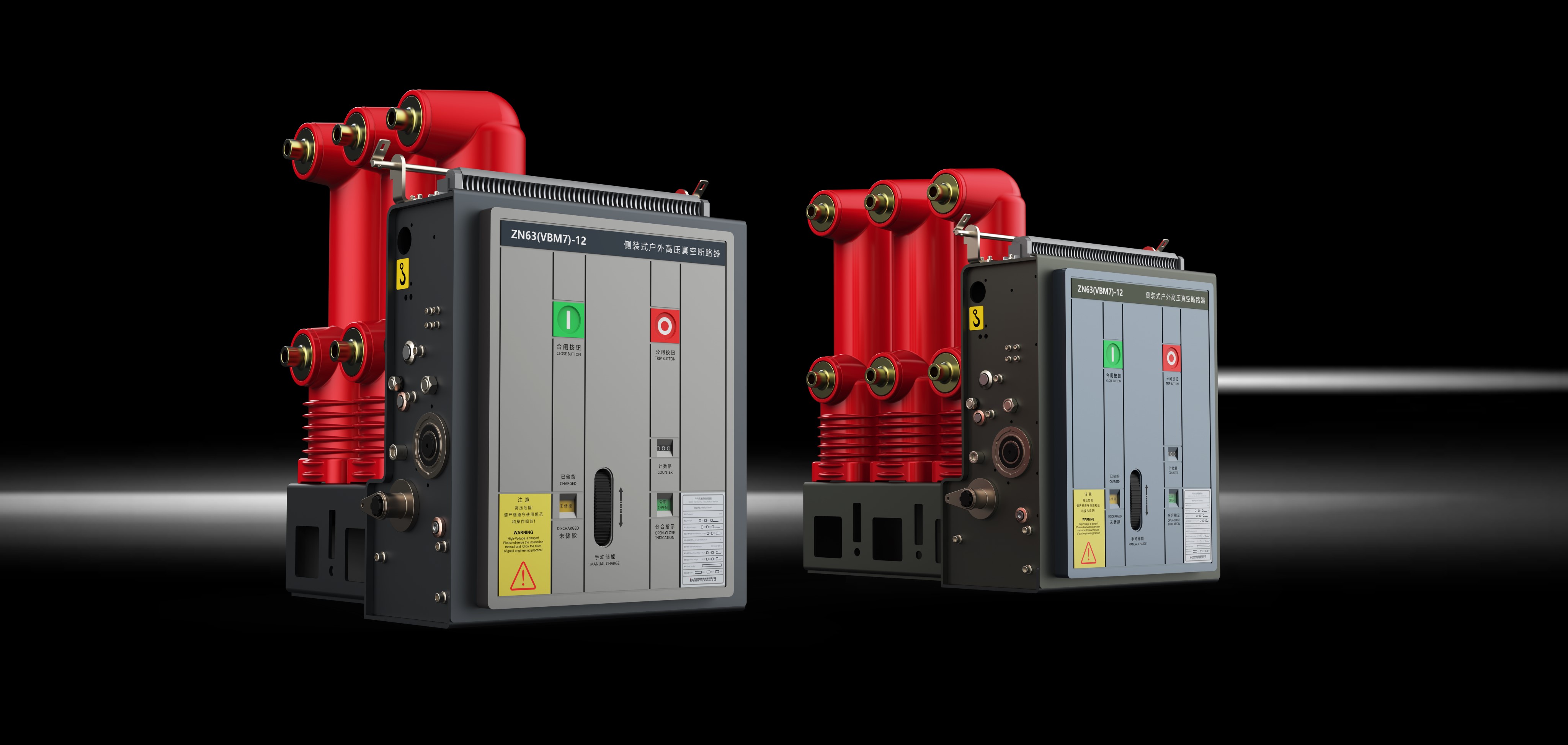
VZO-12系列户外高压真空断路器 | 卖方: 839459 | 户外高压真空断路器: VZO-12系列型户外高压真空断路器(以下简称断路器)为额定电压12kV,三相交流50Hz的户外配电设备。它采用真空灭弧和SF6气体作为绝缘介质,是MVXOZ-12型柱上真... |
 |
真空断路器 | 卖方: 839459 | 固封式户内高压真空断路器: VZCN-12系列户内高压真空断路器,额定电压为12KV,三相交流50Hz的户内高压开关设备,适用于发电厂、变电所及工矿企业输配电系统的控制或保护开关,尤其适用于高海... |
 |
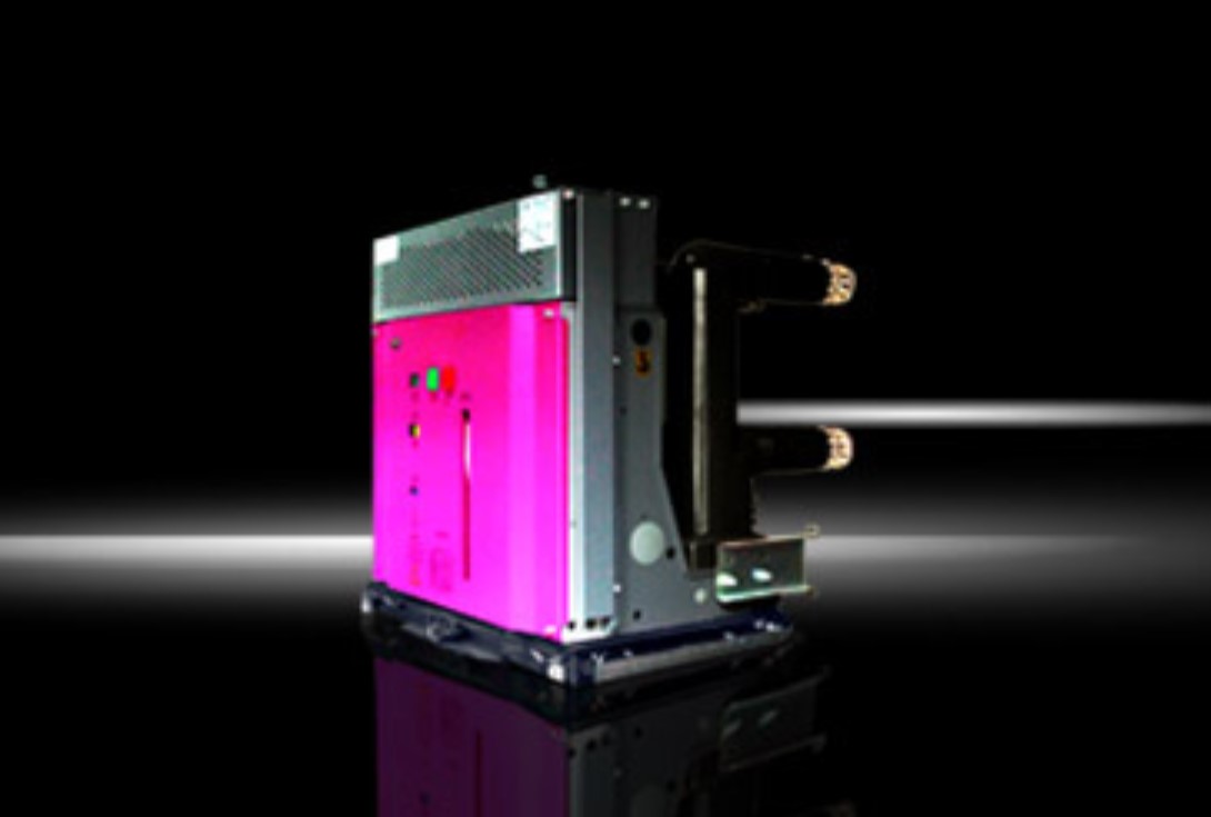
真空断路器 | 卖方: 839459 | 侧装式户内高压真空断路器: 真空断路器通常可分多个电压等级,低压型一般用于防爆电气使用,例如煤矿等等。其额定电流达到5000A,开断电流达到50kA的较好水平,并已发展到电压达35kV等级。 ... |
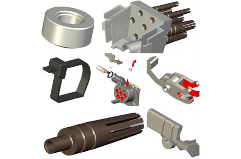 |
DELIVER MOLDING MECHANICAL DESIGNS SYSTEMATICALLY | 卖方: GreensTone (Shenzhen) Electronics Co., Limited | GreensTone mechanical design engineers will work with your team to design and test the best solut... |
