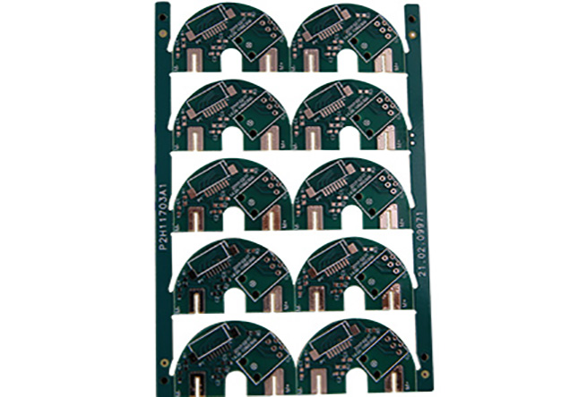
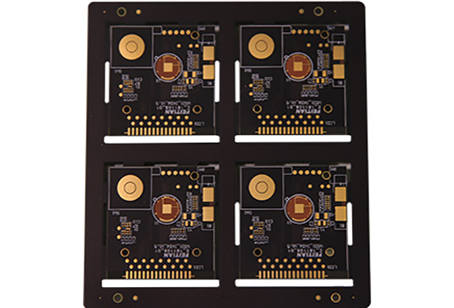
Double side 8 layers HDI PCB assembly manufacturing


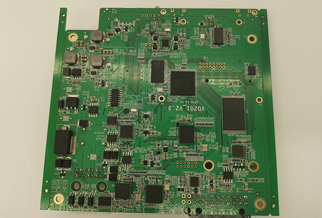
Double side 8 layers HDI PCB assembly manufacturing
● 4 YAMAHA High-speed SMT Lines
● 6 million daily SMT placements capability
● 400,000 daily DIP placements capability
● 500×600 mm Maximum Board Size
● 0.25"x 0.25" Minimum Board Size
● 450 mm Max. Width for Wave-Solder
● Passives Components Down to 0201 Size BGA and VFBGA Leadless Chip Carrier/CSP Double-Sided SMT AssemblyFine Pitch to 08 Mil BGA Repair and ReballPart Removal and Replacement
SMT and DIP/X-RAY Inspection/AOI Testing/In-circuit-test (ICT)/Flying Probe/Function Test/Burn-in/Finished products assembly
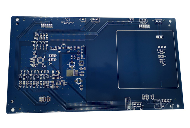
What is a high frequency (HF) PCB?
Electronic devices with high frequency is the developing tendency nowadays, especially in wireless network. Satellite communications are developing rapidly, and information products are moving towards high speeds and high frequency. Accordingly, developing new products always requires high-frequency substrates. These communication products, like satellite systems, mobile s, must use high-frequency PCBs.
The characteristics of high frequency PCB.
It has special materials requirements for the high frequency boards for wireless applications and data rates in the high GHz range:
In general, the high frequency can be defined as a frequency above 1 GHz. Currently, PTFE materials are widely used in high-frequency PCB manufacturing, also known as Teflon, and their frequencies are usually higher than 5 GHz. In addition, FR4 or PPO substrates can be used for product frequencies between 1 GHz and 10 GHz.
Check our HF PCB capabilities by reviewing below table:
|
Feature |
Capability |
|
Quality Grade |
Standard IPC 2 |
|
Number of Layers |
2 - 20layers |
|
Build Time |
2days - 5weeks |
|
Material |
RO4003C, RO4350B, Ro3003, Ro3010, RT5880 etc. |
|
Board Thickness |
|
|
Copper Weight(Finished) |
|
|
Min Tracing/Spacing |
3mil/3mil |
|
Solder Mask Sides |
As per the file |
|
Solder Mask Color |
Green, White, Blue, Black, Red, Yellow |
|
Silkscreen Sides |
As per the file |
|
Silkscreen Color |
White, Black, Yellow |
|
Surface Finish |
Electroless nickel/immersion gold (ENIG) - RoHS |
|
Immersion silver - RoHS |
|
|
Immersion tin - RoHS |
|
|
Organic solderability preservatives - RoHS |
|
|
Min Annular Ring |
4mil |
|
Min Drilling Hole Diameter |
6mil |
|
Impedance tolerance |
±10% |
|
Other Techniques |
Peelable solder mask |
|
Gold fingers |
|
|
Carbon oil |
|
|
Countersink holes |
Let’s start to discuss your pcb boardtoday?Just click your favorite button in the right side.
Send product request
Other supplier products
 |
8 layer 1mm HDI PCB 0 gap | 8 layer 1mm HDI PCB 0 gap 8 layer PCB,0 gap PCB,1mm PCB 1)Thickness: 0.1mm-5mm 2)Minimum linewidth:0.075mm/3mil 3)Minimum gap:0.065/2.8mil 4)Minimu... |
 |
high frequency printed circuit board production, gerber file for quote, competitive price | , gerber file for quote, competitive price Brand Name: HK CT TECH OEM PCB Model Number: Double sided, Base Material: FR4,Rogers,Aluminum Copper Thi... |
 |
OEM special design 0.15mm ultrathin double side rigid PCB 4 layers | OEM special design 0.15mm ultrathin double side rigid PCB4 layers OEM special design PCB,Ultrathin PCB )Thickness: 0.1mm-5mm 2)Minimum linewidth:0.... |
 |
Fast supply electric circuit board assembly manufacturer | Fast supply electric circuit board assemblymanufacturer 4 YAMAHA High-speed SMT Lines 6 million daily SMT placements capability 400,000 daily DIP p... |
 |
SMT DIP best quality 6 layers 0201 PCB assembly | SMT DIP best quality 6 layers 0201 PCB assembly SMT PCBA,DIP PCBA ● 4 YAMAHA High-speed SMT Lines ● 6 million daily SMT placements capability ● 400... |