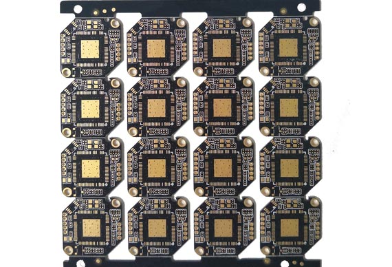
PLATED THROUGH HOLE PCB / PTH PCB


Speedapcb - The printed circuit board manufacturersin China, established in 2014, is located in Changsha, Hunan Province. The company focuses on high-speed PCB design, printed circuit board manufacturing, SMT welding processing, and supply chain services. Products are widely used in communications equipment, computers and network equipment, consumer electronics, automotive electronics, industrial control, new energy, rail transportation, and other industries.
There are three common types of drilled holes in the printed circuit board: pcb through hole plating, blind via hole, and buried pcb via hole. Therefore, PCBs are classified according to drilling methods and can be divided into pth hole in pcb, pcb via plating, pth board, pcb board with holes, through hole pcb assemblyand pcb hole plating.
PTH is the most common drilling method, and it is common in various types of PCBs. SPEEDAPCB has been focusing on the production of various PTH (plated through hole PCB-PTH PCB), buried via hole PCB and blind via hole PCB.
HAVE A QUESTION OR REQUEST?
Click below, we’ll be happy to assist.
Drilling Method of Plated Through Hole PCB
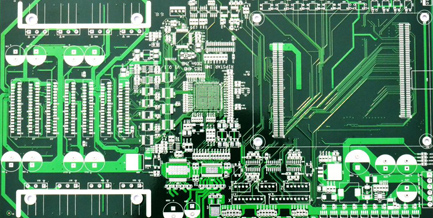
Plated Through Hole, the copper foil lines between conductive patterns in different layers of the circuit board are connected or connected with this type of hole, but the copper legs of the component lead or other reinforced materials cannot be inserted. The PCB is formed by the accumulation of many copper foil layers. The copper foil layers cannot communicate with each other because each layer of copper foil is covered with an insulating layer, so they need to rely on via for signal connection.
The through hole of the circuit board must pass through the plug hole to meet the customer's needs. In changing the traditional aluminum sheet plugging process, the solder mask and plug hole on the circuit board surface are completed with a white net to make its production more stable and the quality more reliable , More perfect to use. The vias help the circuits to be connected to each other. With the rapid development of the electronics industry, higher requirements are also placed on the PCB manufacturing process and surface mount technology. The plugging process for vias came into being, and at the same time, it must meet the following requirements:
- The through hole must have a solder resist ink plug hole, opaque, no tin rings and beads, and must be flat.
Through-hole boards are common in all fields and are one of the most common PCBs.
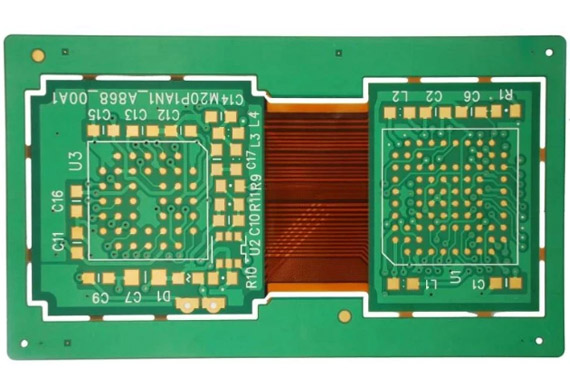
Generally, the mobile board or PDA board has a board that uses a combination of blind and buried holes. The buried hole can reduce the probability of signal interference, maintain the continuity of the transmission line's characteristic impedance, and save routing space. Circuit board design. This type of board requires high technical content and accurate accuracy, so relatively speaking, the requirements for factory equipment are much higher than ordinary multilayer boards, and the cost of such circuit boards will be much higher than ordinary Shelf should be high.
Parameters of Plated Through Hole PCB
|
Items |
||
|
Max board size |
580X700mm |
|
|
Boar Material |
FR-4,Aluminum, High Tg FR4,CEM3,etc. |
|
|
Min trace width/ space (inner layer) |
4mil/4mil(0.1mm/0.1mm) |
|
|
Min PAD (inner layer) |
5 mil(0.13mm) |
|
|
Min thickness(inner layer) |
4 mil(0.1mm) |
|
|
Inner copper thickness |
||
|
Outer copper thickness |
||
|
Finished board thickness |
||
|
±0.10 mm |
±0.10 mm |
|
|
Board thickness tolerance control |
±10% |
±10% |
|
±10% |
±10% |
|
|
Inner layer treatment |
brown oxidation |
|
|
Layer count Capability |
1-30 LAYER |
|
|
alignment between ML |
±2mil |
|
|
Drill hole diameter |
||
|
Aspect ratio of plated hole |
10:01 |
|
|
Hole precision |
±2 mil(±0.05mm) |
|
|
tolerance for Slot |
±3 mil(±0.75mm) |
|
|
Hole diameter tolerance(PTH) |
±3 mil(±0.075mm) |
|
|
Hole diameter tolerance(NPTH) |
±1mil(±0.025mm) |
|
|
Max Aspect Ratio for PTH |
8:01 |
|
|
Hole wall copper thickness |
15-50um |
|
|
Alignment of outer layers |
4mil/4mil |
|
|
Min trace width/space for outer layer |
4mil/4mil |
|
|
Tolerance of Etching |
+/-10% |
|
|
Thickness of solder mask |
on trace |
|
|
Thickness of solder mask |
at trace corner |
≥0.2mil(5um) |
|
Hardness of solder mask |
On base material |
≤+1.2mil |
|
6H |
Finished thickness |
|
|
Alignment of solder mask film |
±2mil(+/-50um) |
|
|
Min width of solder mask bridge |
4mil(100um) |
|
|
Max hole with solder plug |
||
|
Surface treatment |
HAL (Lead or Lead free), immersion Gold, Immersion Nickel, Electric Gold finger, plated Gold, OSP, Immersion Silver.carbon oil,etc. |
|
|
Max Nickel thickness for Gold finger |
280u"(7um) |
|
|
Max gold thickness for Gold finger |
30u"(0.75um) |
|
|
Nickel thickness in Immersion Gold |
120u"/240u"(3um/6um) |
|
|
Gold thickness in Immersion Gold |
2u"/6u"(0.05um/0.15um) |
|
|
Impedance control and its tolerance |
50±10%,75±10%,100±10% 110±10% |
|
|
Trace Anti-stripped strength |
≥61B/in(≥107g/mm) |
|
|
bow and twist |
||
Send product request
Other supplier products
 |
Military PCB Manufacturer & Assembly | Today, printed circuit boards are commonly used in the military and aerospace industries. Military and aerospace products require printed circuit b... |
|
|
PLATED THROUGH HOLE PCB / PTH PCB | Speedapcb - The printed circuit board manufacturersin China, established in 2014, is located in Changsha, Hunan Province. The company focuses on h... |
 |
OSP PCB - PRINTED CIRCUIT BOARD | OSP differs from other surface treatment processes in that it functions as a barrier layer between copper and air; in short, OSP is a chemically gr... |
 |
A NEW TYPE OF WIRE BOARD——RIGID FLEX PCB | Speedapcb - The PCB design companyin China, established in 2014, is located in Changsha, Hunan Province. The company focuses on high-speed PCB desi... |
 |
Medical PCB Manufacturer & Assembly | Electronics makes a significant contribution to the health-the nursing industry, as a diagnostic, monitoring, and treatment device. As the developm... |