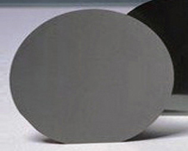
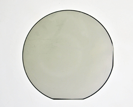
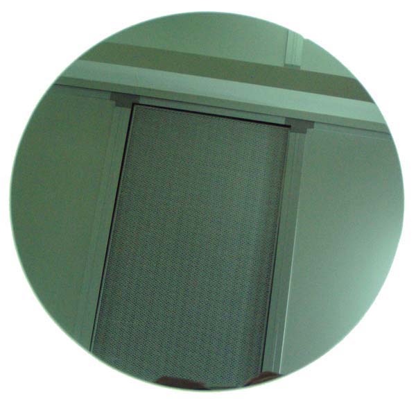
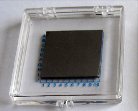
Ge(Germanium)Wafer
Germanium blank or window are used in night vision and thermographic imaging solutions for commercial security, fire fighting and industrial monitoring equipment. Also, they are used as filters for analytical and measuring equipment, windows for remote temperature measurement, and mirrors for lasers.
Thin Germanium substrates are used in III-V triple-junction solar cells and for power Concentrated PV (CPV) systems.
Other supplier products
|
|
SiC(Silicon Carbide)Wafer |
PWAM offers semiconductor materials,SiC substate for GaN epitaxy device,power devices, high-temperature device and optoelectron
PWAM offers semic... |
|
|
Silicon Epitaxial Wafer |
Epitaxy is the process of depositing a thin layer on substrate, Epitaxy layer can be as the same as the basis(Si/Si) or different with the basis (S... |
|
|
Semiconductor wafer |
|
|
|
CZT Wafer |
CdZnTe (Cadmium Zinc Telluride,CZT) is a new semiconductor, which enables to convert radiation to electron effectively, it is mainly used in infrar... |
|
|
Ge(Germanium)Wafer |
Germanium blank or window are used in night vision and thermographic imaging solutions for commercial security, fire fighting and industrial monito... |
供应产品
Same products


