GaAs (Gallium Arsenide) Wafers
PWAM Develops and manufactures compound semiconductor substrates-gallium arsenide crystal and wafer.We has used advanced crystal growth technology,vertical gradient freeze(VGF) and GaAs wafer processing technology,established a production line from crystal growth, cutting, grinding to polishing processing and built a 100-class clean room for wafer cleaning and packaging. Our GaAs wafer include 2~6 inch ingot/wafers for LED,LD and Microelectronics applications.We are always dedicated to improve the quality of currently substates and develop large size substrates.
Other supplier products
|
|
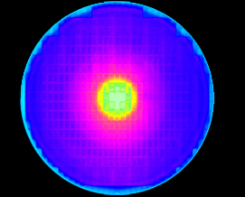
Semiconductor wafer |
|
|
|
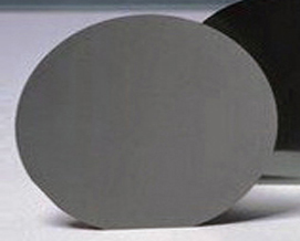
Ge(Germanium)Wafer |
Germanium blank or window are used in night vision and thermographic imaging solutions for commercial security, fire fighting and industrial monito... |
|
|
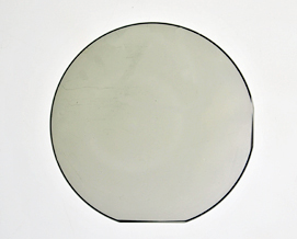
SiC(Silicon Carbide)Wafer |
PWAM offers semiconductor materials,SiC substate for GaN epitaxy device,power devices, high-temperature device and optoelectron
PWAM offers semic... |
|
|
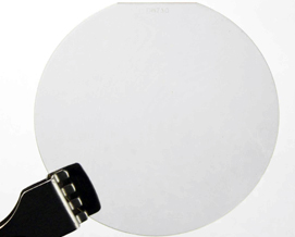
GaAs (Gallium Arsenide) Wafers |
PWAM Develops and manufactures compound semiconductor substrates-gallium arsenide crystal and wafer.We has used advanced crystal growth technology,... |
|
|
GaN(Gallium Nitride) Wafer |
GaN Wafer:2”(50.8mm),14mm*15mm;10mm*10mm;5mm*5mm, Free standing substrate, epi-ready
GaN Template(GaN-on-Sapphire):2"
GaN Epitaxial Wa... |
供应产品
Same products