|
|
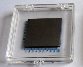
SiC(Silicon Carbide)Wafer |
PWAM offers semiconductor materials,SiC substate for GaN epitaxy device,power devices, high-temperature device and optoelectron
PWAM offers semic... |
|
|
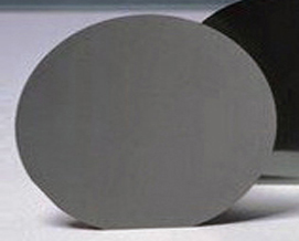
Semiconductor wafer |
|
|
|
CZT Wafer |
CdZnTe (Cadmium Zinc Telluride,CZT) is a new semiconductor, which enables to convert radiation to electron effectively, it is mainly used in infrar... |
|
|
Ge(Germanium)Wafer |
Germanium blank or window are used in night vision and thermographic imaging solutions for commercial security, fire fighting and industrial monito... |
|
|
Silicon Epitaxial Wafer |
Epitaxy is the process of depositing a thin layer on substrate, Epitaxy layer can be as the same as the basis(Si/Si) or different with the basis (S... |
|
|
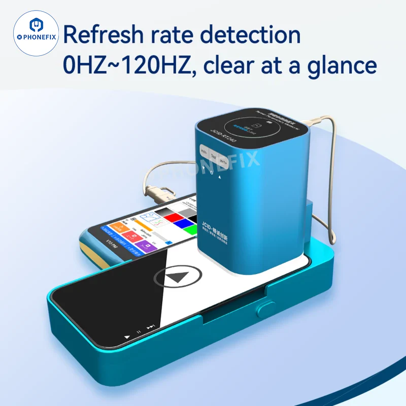
JCID RT240 Screen Resolution Refresh Rate Parameters Measurer |
Seller: PHONEFIX technology Co.,Ltd |
JCID RT240 Screen Parameters Measurer for Mobile Phone/iPhone Display Resolution and Refresh Rate... |
|
|
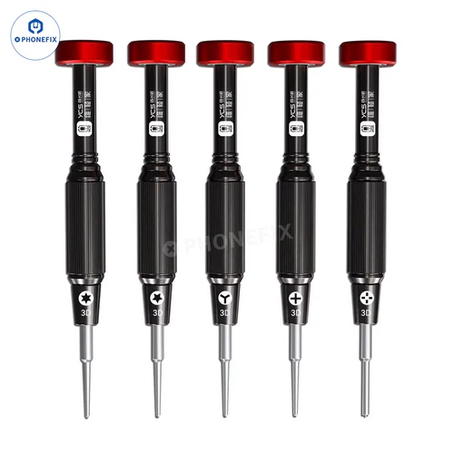
IKS-T05 ZD Skrevdrever Network 5-In-1 Magnetic Bits Disassembly Tool |
Seller: PHONEFIX technology Co.,Ltd |
YCS-T05 5-in-1 3D Screwdriver set with 5 pieces magnetic extra-hard bit for assembling/disassembl... |
|
|
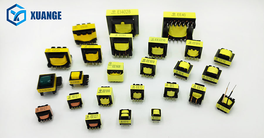
ee8.3-ee60 transformer | transformer manufacturers |
Seller: XuanGe Electronics Manufacturer |
EE model:EE8.3, EE10/11, EE13, EE16, EEL16, EE19, EE20, EE22, EE25, EE25.4, EE30, EE35, EE40, EE4... |
|
|
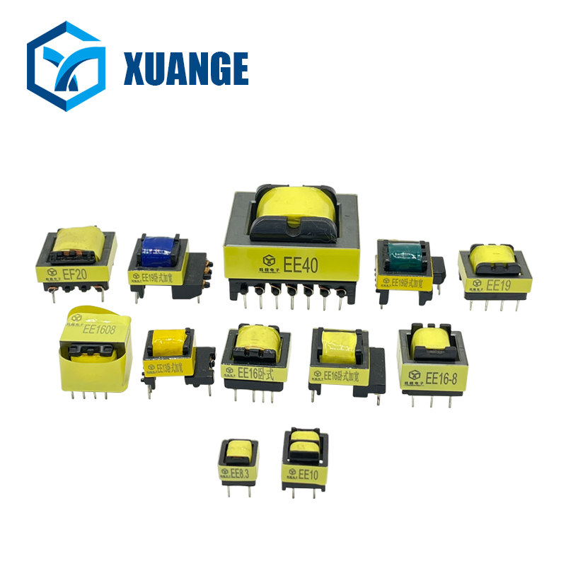
ee8.3-ee60 transformer | transformer manufacturers |
Seller: XuanGe Electronics Manufacturer |
EE model:EE8.3, EE10/11, EE13, EE16, EEL16, EE19, EE20, EE22, EE25, EE25.4, EE30, EE35, EE40, EE4... |
|
|
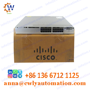
Cisco Catalyst WS-C3850-12S-S Layer 3 Switch |
Seller: 840499 |
Features: Auto-negotiation, ARP support, trunking, VLAN support, auto-uplink (auto MDI/MDI-X), IG... |