

Semiconductor wafer


在线联系供应商
Other supplier products
|
|
Semiconductor wafer | |
 |
Silicon Epitaxial Wafer | Epitaxy is the process of depositing a thin layer on substrate, Epitaxy layer can be as the same as the basis(Si/Si) or different with the basis (S... |
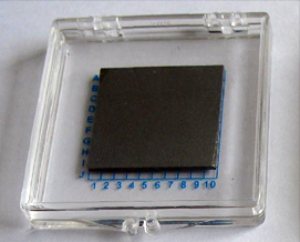 |
CZT Wafer | CdZnTe (Cadmium Zinc Telluride,CZT) is a new semiconductor, which enables to convert radiation to electron effectively, it is mainly used in infrar... |
 |
GaN(Gallium Nitride) Wafer | GaN Wafer:2”(50.8mm),14mm*15mm;10mm*10mm;5mm*5mm, Free standing substrate, epi-ready GaN Template(GaN-on-Sapphire):2" GaN Epitaxial Wa... |
 |
SiC(Silicon Carbide)Wafer | PWAM offers semiconductor materials,SiC substate for GaN epitaxy device,power devices, high-temperature device and optoelectron PWAM offers semic... |
Same products
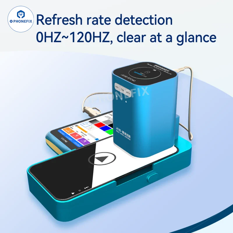 |
JCID RT240屏幕分辨率刷新率参数测量仪 | 卖方: 深圳市维客修科技有限公司 | JCID RT240屏幕参数测量仪,专为手机/iPhone设计,可精准测量显示分辨率与刷新率。 |
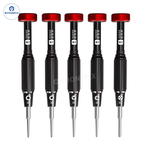 |
YCS-T05 3D 螺丝刀套装 5 合 1 磁性批头拆卸工具 | 卖方: 深圳市维客修科技有限公司 | YCS-T05 5合1 3D螺丝刀套装带5件磁性超硬钻头用于组装/拆卸iPhone 16/15/14/13/12/11/X-6、手机、Pad、笔记本电脑平板电脑、相机等。 YCS-T05 3D螺... |
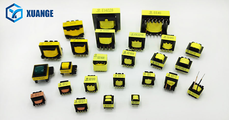 |
EE type transformer | 卖方: 炫格电子制造商 | EE型号: EE8.3、EE10/11、EE13、EE16、EEL16、EE19、EE20、EE22、EE25、EE25.4、EE30、EE35、EE40、EE41/33、EE42/15 支持定制 |
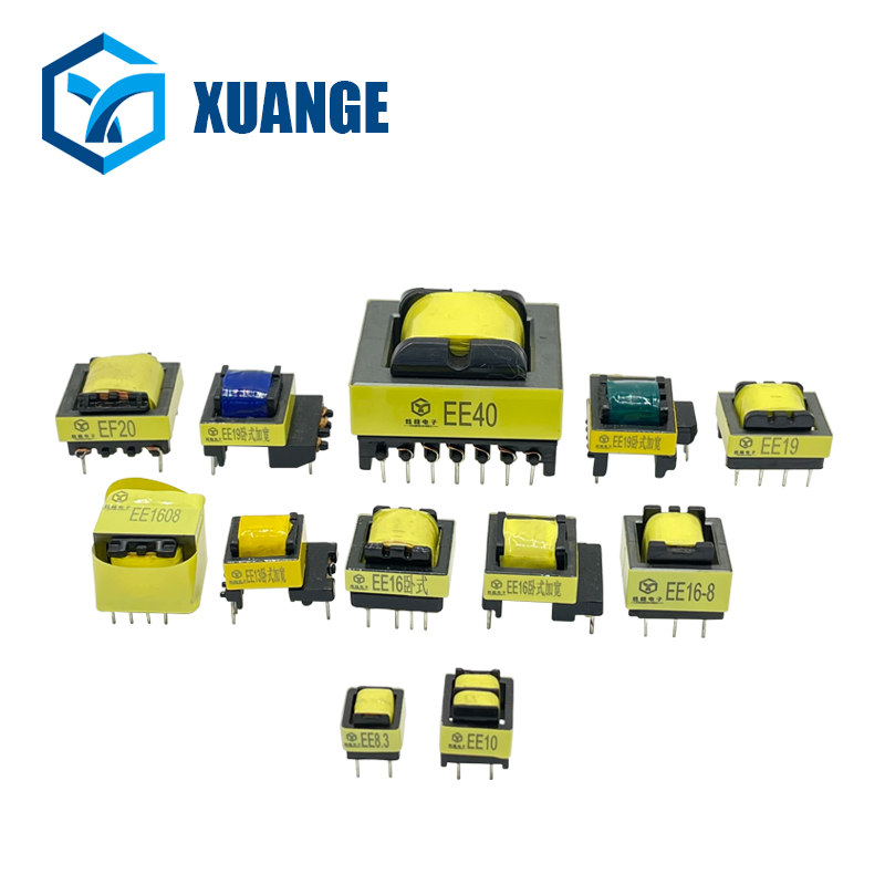 |
EE type transformer | 卖方: 炫格电子制造商 | EE型号: EE8.3、EE10/11、EE13、EE16、EEL16、EE19、EE20、EE22、EE25、EE25.4、EE30、EE35、EE40、EE41/33、EE42/15 支持定制 |
 |
Cisco Catalyst WS-C3850-12S-S Layer 3 Switch | 卖方: 840499 | Features: Auto-negotiation, ARP support, trunking, VLAN support, auto-uplink (auto MDI/MDI-X), IG... |
